MULTIPROTOCOL SERIAL COMMUNICATIONS INTERFACE (SCI-M)
MULTIPROTOCOL SERIAL COMMUNICATIONS INTERFACE (Cont’d)
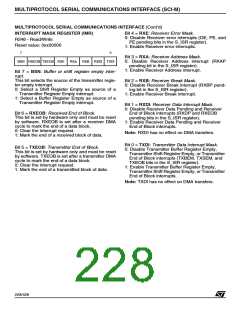
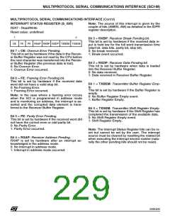
INTERRUPT STATUS REGISTER (S_ISR)
R247 - Read/Write
Note: The source of this interrupt is given by the
couple of bits (AMEN, AM) as detailed in the IDPR
register description.
Reset value: undefined
7
0
Bit 3 = RXBP: Receiver Break Pending bit.
This bit is set by hardware if the received data in-
put is held low for the full word transmission time
(start bit, data bits, parity bit, stop bit).
0: No break received.
OE
FE
PE RXAP RXBP RXDP TXBEM TXSEM
Bit 7 = OE: Overrun Error Pending.
This bit is set by hardware if the data in the Receiv-
er Buffer Register was not read by the CPU before
the next character was transferred into the Receiv-
er Buffer Register (the previous data is lost).
0: No Overrun Error.
1: Break event occurred.
Bit 2 = RXDP: Receiver Data Pending bit.
This bit is set by hardware when data is loaded
into the Receiver Buffer Register.
0: No data received.
1: Data received in Receiver Buffer Register.
1: Overrun Error occurred.
Bit 6 = FE: Framing Error Pending bit.
This bit is set by hardware if the received data
word did not have a valid stop bit.
0: No Framing Error.
Bit 1 = TXBEM: Transmitter Buffer Register Emp-
ty.
This bit is set by hardware if the Buffer Register is
empty.
0: No Buffer Register Empty event.
1: Buffer Register Empty.
1: Framing Error occurred.
Note: In the case where a framing error occurs
when the SCI is programmed in address mode
and is monitoring an address, the interrupt is as-
serted and the corrupted data element is trans-
ferred to the Receiver Buffer Register.
Bit 0 = TXSEM: Transmitter Shift Register Empty.
This bit is set by hardware if the Shift Register has
completed the transmission of the available data.
0: No Shift Register Empty event.
Bit 5 = PE: Parity Error Pending.
This bit is set by hardware if the received word did
not have the correct even or odd parity bit.
0: No Parity Error.
1: Shift Register Empty.
1: Parity Error occurred.
Note: The Interrupt Status Register bits can be re-
set but cannot be set by the user. The interrupt
source must be cleared by resetting the related bit
when executing the interrupt service routine (natu-
rally the other pending bits should not be reset).
Bit 4 = RXAP: Receiver Address Pending.
RXAP is set by hardware after an interrupt ac-
knowledged in the address mode.
0: No interrupt in address mode.
1: Interrupt in address mode occurred.
229/426
9

 STMICROELECTRONICS [ ST ]