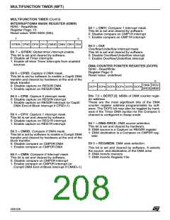
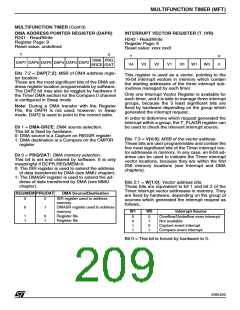
MULTIFUNCTION TIMER (MFT)
MULTIFUNCTION TIMER (Cont’d)
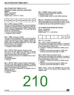
OUTPUT B CONTROL REGISTER (OBCR)
R253 - Read/Write
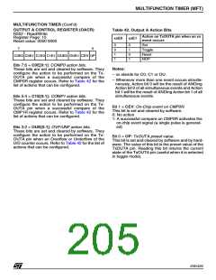
Table 43. Output B Action Bits
Action on the TxOUTB pin when an
xx event occurs
Register Page: 10
xxE0
xxE1
Reset value: 0000 0000 (00h)
0
0
1
1
0
1
0
1
Set
7
0
Toggle
Reset
NOP
C0E0 C0E1 C1E0 C1E1 OUE0 OUE1 OEV 0P
Bits 7:6 = C0E[0:1]: COMP0 Action Bits.
Notes:
These bits are set and cleared by software. They
configure the type of action to be performed on the
TxOUTB output pin when successful compare of
the CMP0R register occurs. Refer to Table 43 for
the list of actions that can be configured.
– xx stands for C0, C1 or OU.
– Whenever more than one event occurs simulta-
neously, Action Bit 0 will be the result of ANDing
Action Bit 0 of all simultaneous events and Action
Bit 1 will be the result of ANDing Action Bit 1 of
all simultaneous events.
Bits 5:4 = C0E[0:1]: COMP1 Action Bits.
These bits are set and cleared by software. They
configure the type of action to be performed on the
TxOUTB output pin when a successful compare of
the CMP1R register occurs. Refer to Table 43 for
the list of actions that can be configured.
Bit 1 = OEV: On-Chip event on OVF/UNF.
This bit is set and cleared by software.
0: No action
1: An underflow/overflow activates the on-chip
event signal (a single pulse is generated)
Bits 3:2 = OUE[0:1]: OVF/UNF Action Bits.
These bits are set and cleared by software.They
configure the type of action to be performed on the
TxOUTB output pin when an Overflow or Under-
flow on the U/D counter occurs. Refer to Table 43
for the list of actions that can be configured.
Bit 0 = OP: TxOUTB preset value.
This bit is set and cleared by software and by hard-
ware. The value of this bit is the preset value of the
TxOUTB pin. Reading this bit returns the current
state of the TxOUTB pin (useful when it is selected
in toggle mode).
206/426
9

 STMICROELECTRONICS [ ST ]