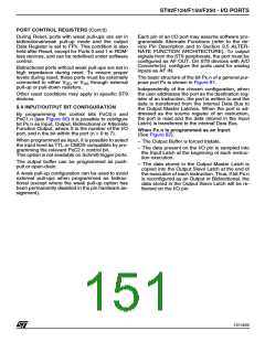
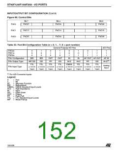
ST92F124/F150/F250 - I/O PORTS
9.5 ALTERNATE FUNCTION ARCHITECTURE
Each I/O pin may be connected to three different
types of internal signal:
9.5.3 Pin Declared as an Alternate Function
Output
– Data bus Input/Output
– Alternate Function Input
– Alternate Function Output
9.5.1 Pin Declared as I/O
The user must select the AF OUT configuration
using the PxC2, PxC1, PxC0 bits. Several Alter-
nate Function outputs may drive a common pin. In
such case, the Alternate Function output signals
are logically ANDed before driving the common
pin. The user must therefore enable the required
Alternate Function Output by software.
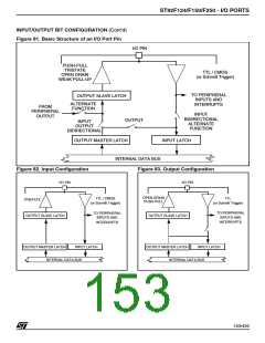
A pin declared as I/O, is connected to the I/O buff-
er. This pin may be an Input, an Output, or a bidi-
rectional I/O, depending on the value stored in
(PxC2, PxC1 and PxC0).
WARNING: When a pin is connected both to an al-
ternate function output and to an alternate function
input, it should be noted that the output signal will
always be present on the alternate function input.
9.5.2 Pin Declared as an Alternate Function
Input
A single pin may be directly connected to several
Alternate Function inputs. In this case, the user
must select the required input mode (with the
PxC2, PxC1, PxC0 bits) and enable the selected
Alternate Function in the Control Register of the
peripheral. No specific port configuration is re-
quired to enable an Alternate Function input, since
the input buffer is directly connected to each alter-
nate function module on the shared pin. As more
than one module can use the same input, it is up to
the user software to enable the required module
as necessary. Parallel I/Os remain operational
even when using an Alternate Function input. The
exception to this is when an I/O port bit is perma-
nently assigned by hardware as an A/D bit. In this
case , after software programming of the bit in AF-
OD-TTL, the Alternate function output is forced to
logic level 1. The analog voltage level on the cor-
responding pin is directly input to the A/D (See Fig-
ure 86).
9.6 I/O STATUS AFTER WFI, HALT AND RESET
The status of the I/O ports during the Wait For In-
terrupt, Halt and Reset operational modes is
shown in the following table. The External Memory
Interface ports are shown separately. If only the in-
ternal memory is being used and the ports are act-
ing as I/O, the status is the same as shown for the
other I/O ports.
Ext. Mem - I/O Ports
Mode
I/O Ports
P1, P2, P6,
P9[7:2] *
P0
High Imped-
anceornext
address
(depending
on the last
memory op-
eration per-
formed on
Port)
Next
Address
Not Affected (clock
outputs running)
WFI
Figure 86. A/D Input Configuration
I/O PIN
High Imped-
ance
Next
Address
Not Affected (clock
outputs stopped)
TOWARDS
ADC CONVERTER
HALT
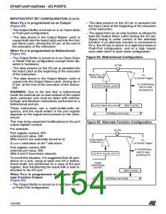
TRISTATE
GND
Bidirectional Weak
Pull-up (High im-
pedance when dis-
abled in
Alternate function push-
pull (ROMless device)
RESET
INPUT
hardware).
OUTPUT SLAVE LATCH
BUFFER
* Depending on device
OUTPUT MASTER LATCH
INPUT LATCH
INTERNAL DATA BUS
155/426
9

 STMICROELECTRONICS [ ST ]