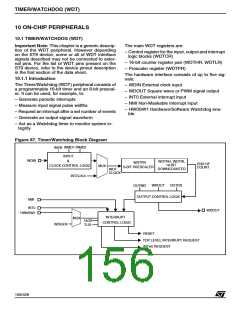
ST92F124/F150/F250 - I/O PORTS
INPUT/OUTPUT BIT CONFIGURATION (Cont’d)
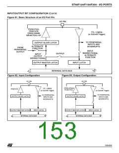
When Px.n is programmed as an Output:
– The data present on the I/O pin is sampled into
the Input Latch at the beginning of the execution
of the instruction.
(Figure 83)
– The Output Buffer is turned on in an Open-drain
or Push-pull configuration.
– The signal from an on-chip function is allowed to
load the Output Slave Latch driving the I/O pin.
Signal timing is under control of the alternate
function. If no alternate function is connected to
Px.n, the I/O pin is driven to a high level when in
Push-Pull configuration, and to a high imped-
ance state when in open drain configuration.
– The data stored in the Output Master Latch is
copied both into the Input Latch and into the Out-
put Slave Latch, driving the I/O pin, at the end of
the execution of the instruction.
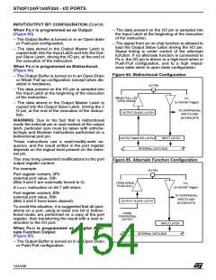
When Px.n is programmed as Bidirectional:
(Figure 84)
Figure 84. Bidirectional Configuration
– The Output Buffer is turned on in an Open-Drain
or Weak Pull-up configuration (except when dis-
abled in hardware).
I/O PIN
– The data present on the I/O pin is sampled into
the Input Latch at the beginning of the execution
of the instruction.
WEAK PULL-UP
OPEN DRAIN
TTL
(or Schmitt Trigger)
– The data stored in the Output Master Latch is
copied into the Output Slave Latch, driving the I/
O pin, at the end of the execution of the instruc-
tion.
TO PERIPHERAL
INPUTS AND
OUTPUT SLAVE LATCH
INTERRUPTS
WARNING: Due to the fact that in bidirectional
mode the external pin is read instead of the output
latch, particular care must be taken with arithme-
tic/logic and Boolean instructions performed on a
bidirectional port pin.
OUTPUT MASTER LATCH
INPUT LATCH
These instructions use a read-modify-write se-
quence, and the result written in the port register
depends on the logical level present on the exter-
nal pin.
INTERNAL DATA BUS
n
n
This may bring unwanted modifications to the port
output register content.
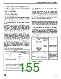
Figure 85. Alternate Function Configuration
For example:
I/O PIN
Port register content, 0Fh
external port value, 03h
(Bits 3 and 2 are externally forced to 0)
OPEN DRAIN
PUSH-PULL
TTL
(or Schmitt Trigger)
A bsetinstruction on bit 7 will return:
Port register content, 83h
external port value, 83h
(Bits 3 and 2 have been cleared).
TO PERIPHERAL
INPUTS AND
OUTPUT SLAVE LATCH
INTERRUPTS
To avoid this situation, it is suggested that all oper-
ations on a port, using at least one bit in bidirec-
tional mode, are performed on a copy of the port
register, then transferring the result with a load in-
struction to the I/O port.
FROM
PERIPHERAL
OUTPUT
INPUT LATCH
When Px.n is programmed as a digital Alter-
nate Function Output:
INTERNAL DATA BUS
(Figure 85)
n
n
n
n
n
n
– The Output Buffer is turned on in an Open-Drain
or Push-Pull configuration.
154/426
9

 STMICROELECTRONICS [ ST ]