ST92F124/F150/F250 - I/O PORTS
9 I/O PORTS
9.1 INTRODUCTION
9.2 SPECIFIC PORT CONFIGURATIONS
ST9 devices feature flexible individually program-
mable multifunctional input/output lines. Refer to
the Pin Description Chapter for specific pin alloca-
tions. These lines, which are logically grouped as
8-bit ports, can be individually programmed to pro-
vide digital input/output and analog input, or to
connect input/output signals to the on-chip periph-
erals as alternate pin functions. All ports can be in-
dividually configured as an input, bi-directional,
output or alternate function. In addition, pull-ups
can be turned off for open-drain operation, and
weak pull-ups can be turned on in their place, to
avoid the need for off-chip resistive pull-ups. Ports
configured as open drain must never have voltage
Refer to the Pin Description chapter for a list of the
specific port styles and reset values.
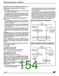
9.3 PORT CONTROL REGISTERS
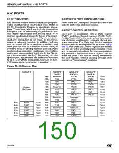
Each port is associated with a Data register
(PxDR) and three Control registers (PxC0, PxC1,
PxC2). These define the port configuration and al-
low dynamic configuration changes during pro-
gram execution. Port Data and Control registers
are mapped into the Register File as shown in Fig-
ure 79. Port Data and Control registers are treated
just like any other general purpose register. There
are no special instructions for port manipulation:
any instruction that can address a register, can ad-
dress the ports. Data can be directly accessed in
the port register, without passing through other
memory or “accumulator” locations.
on the port pin exceeding V (refer to the Electri-
DD
cal Characteristics section). Depending on the
specific port, input buffers are software selectable
to be TTL or CMOS compatible, however on Sch-
mitt trigger ports, no selection is possible.
Figure 79. I/O Register Map
GROUP E
GROUP F
GROUP F
PAGE 3
GROUP F
PAGE 43
PAGE 2
Reserved
P3C2
FFh
FEh
FDh
FCh
FBh
FAh
F9h
F8h
F7h
F6h
F5h
F4h
F3h
F2h
F1h
F0h
P7DR
P7C2
P9DR
P9C2
P9C1
P9C0
P8DR
P8C2
P8C1
P8C0
R255
R254
R253
R252
R251
R250
R249
R248
R247
R246
R245
R244
R243
R242
R241
R240
P3C1
P7C1
P3C0
P7C0
Reserved
P2C2
P6DR
P6C2
System
Registers
P2C1
P6C1
P2C0
P6C0
Reserved
P1C2
Reserved
P5C2
E5h
E4h
E3h
E2h
E1h
E0h
P5DR
P4DR
P3DR
P2DR
P1DR
P0DR
R229
R228
R227
R226
R225
R224
P1C1
P5C1
Reserved
P1C0
P5C0
Reserved
P0C2
Reserved
P4C2
P0C1
P4C1
P0C0
P4C0
150/426
9

 STMICROELECTRONICS [ ST ]