ST92F124/F150/F250 - EXTERNAL MEMORY INTERFACE (EXTMI)
EXTERNAL MEMORY INTERFACE REGISTERS (Cont’d)
Bit 1:0 = UAS[1:0]: Upper memory address strobe
stretch.
These two bits contain the number of wait cycles
(from 0 to 3) to add to the System Clock to stretch
AS during external upper memory block accesses
(A21=1). The reset value is 3.
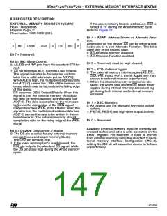
memory block accesses. UDS = 0 adds no addi-
tional wait cycles. UDS = 7 adds the maximum 7
INTCLK cycles (reset condition).
Bit 2:0 = LDS[2:0]: Lower memory data strobe
stretch.
These bits contain the number of INTCLK cycles
to be added automatically to DS for external lower
memory block accesses. LDS = 0 adds no addi-
tional wait cycles, LDS = 7 adds the maximum 7
INTCLK cycles (reset condition).
Caution: The EMR2 register cannot be written
during an interrupt service routine.
WAIT CONTROL REGISTER (WCR)
R252 - Read/Write
Note 1: The number of clock cycles added refers
Register Page: 0
to INTCLK and NOT to CPUCLK.
Reset Value: 0111 1111 (7Fh)
Note 2: The distinction between the Upper memo-
ry block and the Lower memory block allows differ-
ent wait cycles between the first 2 Mbytes and the
second 2 Mbytes, and allows 2 different data
strobe signals to be used to access 2 different
memories.
7
0
0
WDGEN UDS2 UDS1 UDS0 LDS2 LDS1 LDS0
Bit 7 = Reserved, forced by hardware to 0.
Typically, the RAM will be located above address
0x200000 and the ROM below address
0x1FFFFF, with different access times (see Figure
74).
Bit 6 = WDGEN: Watchdog Enable.
For a description of this bit, refer to the Timer/
Watchdog chapter.
Caution: The reset value of the Wait Control Reg-
ister gives the maximum number of Wait cycles for
external memory. To get optimum performance
from the ST9, the user should write the UDS[2:0]
and LDS[2:0] bits to 0, if the external addressed
memories are fast enough.
Caution: Clearing this bit has the effect of setting
the Timer/Watchdog to Watchdog mode. Unless
this is desired, it must be set to “1”.
Bit 5:3 = UDS[2:0]: Upper memory data strobe
stretch.
These bits contain the number of INTCLK cycles
to be added automatically to DS for external upper
149/426
9

 STMICROELECTRONICS [ ST ]