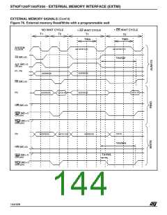
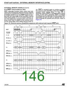
ST92F124/F150/F250 - EXTERNAL MEMORY INTERFACE (EXTMI)
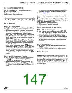
8.3 REGISTER DESCRIPTION
EXTERNAL MEMORY REGISTER 1 (EMR1)
R245 - Read/Write
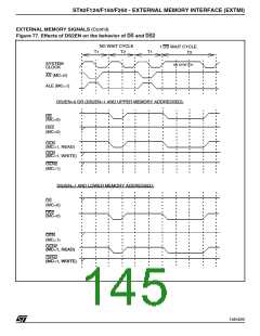
If the upper memory block is addressed, DS2 is
forced to “1” during the whole memory cycle.
Refer to Figure 77
Register Page: 21
Reset value: 1000 0000 (80h)
Bit 4 = ASAF: Address Strobe as Alternate Func-
tion.
7
0
Depending on the device, AS can be either a ded-
icated pin or a port Alternate Function. This bit is
used only in the second case.
X
MC
DS2EN
ASAF
0
ETO
BSZ
X
0: AS Alternate function disabled.
1: AS Alternate Function enabled.
Bit 7 = Reserved.
Bit 6 = MC: Mode Control.
Bit 3 = Reserved, must be kept cleared.
0: AS, DS and RW pins have the standard ST9 for-
mat.
Bit 2 = ETO: External toggle.
1: AS pin becomes ALE, Address Load Enable.
This signal indicates to the external address
latch that a valid address is put on AD[7:0].
When ALE is high, the multiplexed address/data
bus AD[7:0] carries the LSBs of the memory ad-
dress, which must be latched on the falling edge
of this signal.
DS becomes OEN, Output ENable: When this
signal is low, the external memory should put
the data on the multiplexed address/data bus
AD[7:0]. The data is sampled by the microcon-
troller on the rising edge of the OEN signal.
RW pin becomes WEN, Write ENable: when this
signal is low, the multiplexed address/data bus
AD[7:0] carries the data to be written in the ex-
ternal memory. The external memory should
sample the data on the rising edge of the WEN
signal.
0: The external memory interface pins (AS, DS,
DS2, RW, Port0, Port1, Port9) toggle only if an
access to external memory is performed.
1: When the internal memory protection is dis-
abled, the above pins (except DS which never
toggles during internal memory accesses) tog-
gle during both internal and external memory
accesses.
Bit 1 = BSZ: Bus size.
0: All outputs use the standard low-noise output
buffers.
1: P4[7:6], P6[5:4] use high-drive output buffers
Bit 0 = Reserved.
Caution: External memory must be correctly ad-
dressed before and after a write operation on the
EMR1 register. For example, if code is fetched
from external memory using the standard ST9 ex-
ternal memory interface configuration (MC=0),
setting the MC bit will cause the device to behave
unpredictably.
Bit 5 = DS2EN: Data Strobe 2 enable.
0: The DS pin is active for any external memory
access (lower and upper memory block).
The DS2 pin remains high.
1: If the lower memory block is addressed, the
DS2 pin outputs the standard DS signal, while
the DS pin stays high during the whole memory
cycle.
147/426
9

 STMICROELECTRONICS [ ST ]