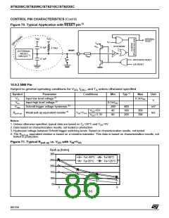
ST6208C/ST6209C/ST6210C/ST6220C
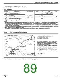
10.9 CONTROL PIN CHARACTERISTICS
10.9.1 Asynchronous RESET Pin
Subject to general operating conditions for V , f
, and T unless otherwise specified.
DD OSC
A
1)
Symbol
Parameter
Conditions
Min
Typ
Max
Unit
V
2)
V
Input low level voltage
0.3xVDD
IL
2)
V
Input high level voltage
0.7xVDD
200
IH
3)
V
Schmitt trigger voltage hysteresis
400
350
730
2.8
mV
kΩ
hys
V
V
V
V
=5V
150
900
DD
DD
DD
DD
4)
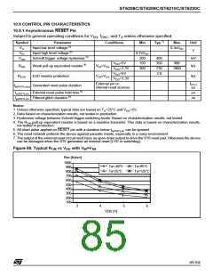
R
Weak pull-up equivalent resistor
V =V
ON
IN
SS
=3.3V
=5V
300
1900
R
ESD resistor protection
V =V
kΩ
ESD
IN
SS
=3.3V
External pin or
internal reset sources
t
CPU
µs
t
Generated reset pulse duration
w(RSTL)out
5)
t
t
External reset pulse hold time
µs
h(RSTL)in
g(RSTL)in
6)
Filtered glitch duration
ns
Notes:
1. Unless otherwise specified, typical data are based on T =25°C and V =5V.
A
DD
2. Data based on characterization results, not tested in production.
3. Hysteresis voltage between Schmitt trigger switching levels. Based on characterization results, not tested.
4. The R
pull-up equivalent resistor is based on a resistive transistor. This data is based on characterization results,
ON
not tested in production.
5. All short pulse applied on RESET pin with a duration below t
can be ignored.
h(RSTL)in
6. The reset network protects the device against parasitic resets, especially in a noisy environment.
7. The output of the external reset circuit must have an open-drain output to drive the ST6 reset pad. Otherwise the device
can be damaged when the ST6 generates an internal reset (LVD or watchdog).
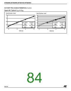
Figure 69. Typical R
vs V with V =V
DD IN SS
ON
Ron [Kohm]
1000
900
800
700
600
500
400
300
Ta=-40°C
Ta=25°C
Ta=95°C
Ta=125°C
200
100
3
4
5
6
VDD [V]
85/104
1

 STMICROELECTRONICS [ ST ]