ST6208C/ST6209C/ST6210C/ST6220C
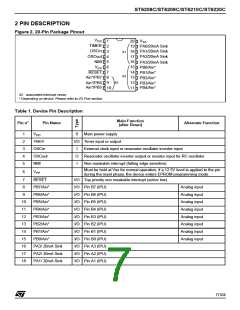
2 PIN DESCRIPTION
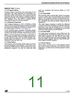
Figure 2. 20-Pin Package Pinout
V
V
DD
1
20
19
18
17
16
15
14
13
12
11
SS
TIMER
OSCin
OSCout
NMI
PA0/20mA Sink
PA1/20mA Sink
PA2/20mA Sink
2
3
it1
it2
4
5
PA3/20mA Sink
PB0/Ain*
V
6
PP
RESET
7
PB1/Ain*
Ain*/PB7
8
PB2/Ain*
it2
9
Ain*/PB6
Ain*/PB5
PB3/Ain*
PB4/Ain*
10
itX associated interrupt vector
* Depending on device. Please refer to I/O Port section.
Table 1. Device Pin Description
Main Function
(after Reset)
Pin n°
Pin Name
Alternate Function
1
2
3
4
5
V
S
Main power supply
DD
TIMER
OSCin
OSCout
NMI
I/O Timer input or output
I
O
I
External clock input or resonator oscillator inverter input
Resonator oscillator inverter output or resistor input for RC oscillator
Non maskable interrupt (falling edge sensitive)
Must be held at Vss for normal operation, if a 12.5V level is applied to the pin
during the reset phase, the device enters EPROM programming mode.
6
V
PP
7
RESET
I/O Top priority non maskable interrupt (active low)
8
PB7/Ain*
I/O Pin B7 (IPU)
Analog input
Analog input
Analog input
Analog input
Analog input
Analog input
Analog input
Analog input
9
PB6/Ain*
I/O Pin B6 (IPU)
10
11
12
13
14
15
16
17
18
PB5/Ain*
I/O Pin B5 (IPU)
PB4/Ain*
I/O Pin B4 (IPU)
PB3/Ain*
I/O Pin B3 (IPU)
PB2/Ain*
I/O Pin B2 (IPU)
PB1/Ain*
I/O Pin B1 (IPU)
PB0/Ain*
I/O Pin B0 (IPU)
PA3/ 20mA Sink
PA2/ 20mA Sink
PA1/ 20mA Sink
I/O Pin A3 (IPU)
I/O Pin A2 (IPU)
I/O Pin A1 (IPU)
7/104
5

 STMICROELECTRONICS [ ST ]