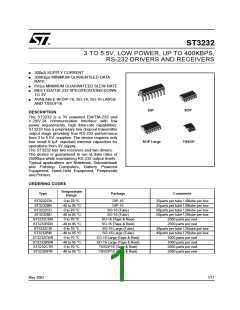
ST3232
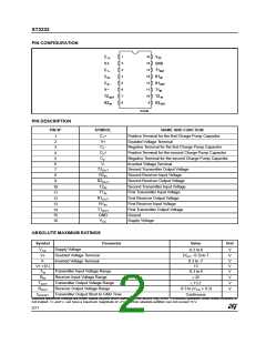
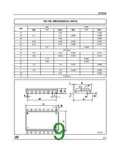
PIN CONFIGURATION
PIN DESCRIPTION
PlN N°
SYMBOL
NAME AND FUNCTION
C +
Positive Terminal for the first Charge Pump Capacitor
1
2
1
V+
Doubled Voltage Terminal
C -
Negative Terminal for the first Charge Pump Capacitor
3
1
C +
Positive Terminal for the second Charge Pump Capacitor
Negative Terminal for the second Charge Pump Capacitor
4
2
C -
5
2
6
V-
Inverted Voltage Terminal
T2
Second Transmitter Output Voltage
7
OUT
R2
Second Receiver Input Voltage
Second Receiver Output Voltage
Second Transmitter Input Voltage
First Transmitter Input Voltage
First Receiver Output Voltage
First Receiver Input Voltage
8
IN
R2
9
OUT
T2
10
11
12
13
14
15
16
IN
T1
IN
R1
OUT
R1
IN
T1
First Transmitter Output Voltage
Ground
OUT
GND
V
Supply Voltage
CC
ABSOLUTE MAXIMUM RATINGS
Symbol
Parameter
Value
Unit
V
Supply Voltage
-0.3 to 6
V
CC
Doubled Voltage Terminal
Inverted Voltage Terminal
(V - 0.3) to 7
V+
V
V
V
V
CC
V-
0.3 to -7
13
V+ +|V-|
T
Transmitter Input Voltage Range
Receiver Input Voltage Range
-0.3 to 6
IN
R
± 25
V
V
V
IN
T
Transmitter Output Voltage Range
Receiver Output Voltage Range
Transmitter Output Short to GND Time
± 13.2
OUT
R
-0.3 to (V + 0.3)
OUT
CC
t
Continuous
SHORT
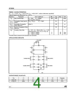
Absolute Maximum Ratings are those values beyond which damage to the device may occur. Functional operation under these condition is
not implied. V+ and V- can have a maximum magnitude of +7V, but their absolute addition can not exceed 13 V.
2/11

 STMICROELECTRONICS [ ST ]