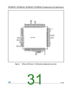
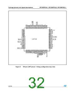
SPC560P34L1, SPC560P34L3, SPC560P40L1, SPC560P40L3 Package pinouts and signal descrip-
2.2.3
Pin multiplexing
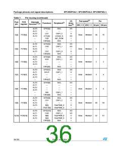
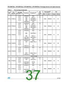
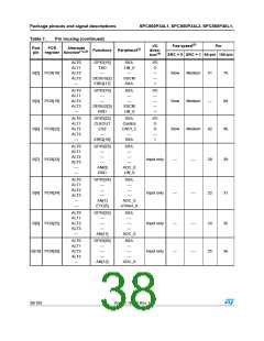
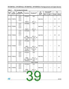
Table 7 defines the pin list and muxing for the SPC560P34/SPC560P40 devices.
Each row of Table 7 shows all the possible ways of configuring each pin, via alternate
functions. The default function assigned to each pin after reset is the ALT0 function.
SPC560P34/SPC560P40 devices provide three main I/O pad types, depending on the
associated functions:
■
■
■
Slow pads are the most common, providing a compromise between transition time and
low electromagnetic emission.
Medium pads provide fast enough transition for serial communication channels with
controlled current to reduce electromagnetic emission.
Fast pads provide maximum speed. They are used for improved NEXUS debugging
capability.
Medium and Fast pads can use slow configuration to reduce electromagnetic emission, at
the cost of reducing AC performance. For more information, see “Pad AC Specifications” in
the device datasheet.
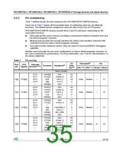
Table 7.
Port
Pin muxing
I/O
Pad speed(5)
Pin
PCR
Alternate
Functions Peripheral(3)
direc-
pin register function(1),(2)
tion(4)
SRC = 0 SRC = 1 64-pin 100-pin
Port A (16-bit)
ALT0
ALT1
GPIO[0]
ETC[0]
SCK
SIUL
eTimer_0
DSPI_2
FCU_0
SIUL
I/O
I/O
I/O
O
A[0]
A[1]
PCR[0]
PCR[1]
ALT2
ALT3
—
Slow
Slow
Medium
Medium
—
—
51
52
F[0]
EIRQ[0]
I
ALT0
ALT1
ALT2
ALT3
—
GPIO[1]
ETC[1]
SOUT
F[1]
SIUL
eTimer_0
DSPI_2
FCU_0
SIUL
I/O
I/O
O
O
EIRQ[1]
I
ALT0
ALT1
ALT2
ALT3
—
GPIO[2]
ETC[2]
—
SIUL
eTimer_0
—
I/O
I/O
—
O
I
A[2]
A[3]
PCR[2]
PCR[3]
A[3]
FlexPWM_0
DSPI_2
MC_RGM
SIUL
Slow
Slow
Medium
Medium
—
57
SIN
—
ABS[0]
EIRQ[2]
I
—
I
ALT0
ALT1
ALT2
ALT3
—
GPIO[3]
ETC[3]
CS0
SIUL
eTimer_0
DSPI_2
I/O
I/O
I/O
O
41
64
B[3]
FlexPWM_0
MC_RGM
SIUL
ABS[1]
EIRQ[3]
I
—
I
Doc ID 16100 Rev 7
35/103

 STMICROELECTRONICS [ ST ]