List of figures
powerSTEP01
List of figures
Figure 1.
Figure 2.
Figure 3.
Figure 4.
Figure 5.
Figure 6.
Figure 7.
Figure 8.
Figure 9.
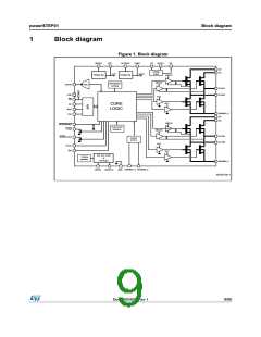
Block diagram. . . . . . . . . . . . . . . . . . . . . . . . . . . . . . . . . . . . . . . . . . . . . . . . . . . . . . . . . . . . 9
Pin connection (top view) . . . . . . . . . . . . . . . . . . . . . . . . . . . . . . . . . . . . . . . . . . . . . . . . . . 17
Typical application schematic - voltage mode . . . . . . . . . . . . . . . . . . . . . . . . . . . . . . . . . . 21
Typical application schematic - current mode. . . . . . . . . . . . . . . . . . . . . . . . . . . . . . . . . . . 21
Charge pump circuitry. . . . . . . . . . . . . . . . . . . . . . . . . . . . . . . . . . . . . . . . . . . . . . . . . . . . . 23
Normal mode and microstepping (128 microsteps) . . . . . . . . . . . . . . . . . . . . . . . . . . . . . . 23
Automatic Full-step switching in Normal mode. . . . . . . . . . . . . . . . . . . . . . . . . . . . . . . . . . 24
Automatic Full-step switching in Boost mode . . . . . . . . . . . . . . . . . . . . . . . . . . . . . . . . . . . 25
Constant speed command examples . . . . . . . . . . . . . . . . . . . . . . . . . . . . . . . . . . . . . . . . . 26
Figure 10. Positioning command examples. . . . . . . . . . . . . . . . . . . . . . . . . . . . . . . . . . . . . . . . . . . . . 27
Figure 11. Motion command examples . . . . . . . . . . . . . . . . . . . . . . . . . . . . . . . . . . . . . . . . . . . . . . . . 27
Figure 12. OSCIN and OSCOUT pin configuration . . . . . . . . . . . . . . . . . . . . . . . . . . . . . . . . . . . . . . . 30
Figure 13. Overcurrent detection - principle scheme . . . . . . . . . . . . . . . . . . . . . . . . . . . . . . . . . . . . . . 31
Figure 14. External switch connection . . . . . . . . . . . . . . . . . . . . . . . . . . . . . . . . . . . . . . . . . . . . . . . . . 34
Figure 15. Device supply pin management . . . . . . . . . . . . . . . . . . . . . . . . . . . . . . . . . . . . . . . . . . . . . 36
Figure 16. Current distortion and compensation . . . . . . . . . . . . . . . . . . . . . . . . . . . . . . . . . . . . . . . . . 40
Figure 17. BEMF compensation curve. . . . . . . . . . . . . . . . . . . . . . . . . . . . . . . . . . . . . . . . . . . . . . . . . 41
Figure 18. Motor supply voltage compensation circuit. . . . . . . . . . . . . . . . . . . . . . . . . . . . . . . . . . . . . 41
Figure 19. Predictive current control . . . . . . . . . . . . . . . . . . . . . . . . . . . . . . . . . . . . . . . . . . . . . . . . . . 43
Figure 20. Non-predictive current control. . . . . . . . . . . . . . . . . . . . . . . . . . . . . . . . . . . . . . . . . . . . . . . 44
Figure 21. Adaptive decay - fast decay tuning. . . . . . . . . . . . . . . . . . . . . . . . . . . . . . . . . . . . . . . . . . . 45
Figure 22. Adaptive decay - switch from normal to slow+ fast decay mode and vice versa . . . . . . . . 46
Figure 23. Fast decay tuning during the falling steps . . . . . . . . . . . . . . . . . . . . . . . . . . . . . . . . . . . . . 47
Figure 24. Current sensing and reference voltage generation. . . . . . . . . . . . . . . . . . . . . . . . . . . . . . . 48
Figure 25. SPI timings diagram . . . . . . . . . . . . . . . . . . . . . . . . . . . . . . . . . . . . . . . . . . . . . . . . . . . . . . 49
Figure 26. Daisy chain configuration . . . . . . . . . . . . . . . . . . . . . . . . . . . . . . . . . . . . . . . . . . . . . . . . . . 50
Figure 27. Command with 3-byte argument. . . . . . . . . . . . . . . . . . . . . . . . . . . . . . . . . . . . . . . . . . . . . 75
Figure 28. Command with 3-byte response. . . . . . . . . . . . . . . . . . . . . . . . . . . . . . . . . . . . . . . . . . . . . 75
Figure 29. Command response aborted . . . . . . . . . . . . . . . . . . . . . . . . . . . . . . . . . . . . . . . . . . . . . . . 75
Figure 30. VFQFPN 11x14x1.0 9 die pads - drawing side view . . . . . . . . . . . . . . . . . . . . . . . . . . . . . 86
Figure 31. VFQFPN 11x14x1.0 9 die pads - drawing bottom view . . . . . . . . . . . . . . . . . . . . . . . . . . . 87
Figure 32. VFQFPN 11x14x1.0 9 die pads - drawing pin identificator . . . . . . . . . . . . . . . . . . . . . . . . . 88
8/90
DocID025022 Rev 1

 STMICROELECTRONICS [ ST ]