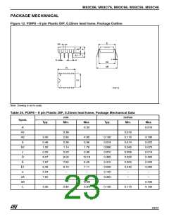
M93C86, M93C76, M93C66, M93C56, M93C46
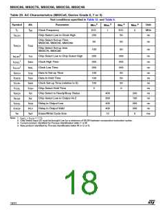
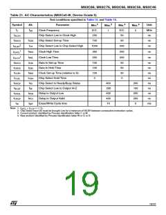
Table 21. AC Characteristics (M93Cx6-W, Device Grade 6)
Test conditions specified in Table 13. and Table 10.
3
3
4
4
Symbol
Alt.
Parameter
Clock Frequency
Unit
MHz
ns
Min.
Max.
Min.
Max.
f
C
f
SK
D.C.
250
1
D.C.
50
2
t
Chip Select Low to Clock High
Chip Select Set-up Time
SLCH
t
t
CSS
100
50
ns
SHCH
2
t
Chip Select Low to Chip Select High
1000
200
ns
t
CS
SLSH
1
t
Clock High Time
350
200
ns
t
SKH
CHCL
1
t
Clock Low Time
250
100
100
100
0
200
50
50
50
0
ns
ns
ns
ns
ns
ns
ns
ns
ns
ms
t
SKL
CLCH
t
t
Data In Set-up Time
DVCH
DIS
DIH
SKS
t
t
Data In Hold Time
CHDX
t
t
t
Clock Set-up Time (relative to S)
Chip Select Hold Time
Chip Select to Ready/Busy Status
Chip Select Low to Output Hi-Z
Delay to Output Low
CLSH
t
CLSL
CSH
t
t
400
200
100
200
200
5
SHQV
SV
t
t
200
400
400
10
SLQZ
DF
t
t
CHQL
PD0
PD1
t
t
Delay to Output Valid
CHQV
t
t
Erase/Write Cycle time
W
WP
Note: 1. t
+ t
CLCH
≥ 1 / f .
C
CHCL
2. Chip Select Input (S) must be brought Low for a minimum of tSLSH between consecutive instruction cycles.
3. Current product: identified by Process Identification letter F or M.
4. New product: identified by Process Identification letter W or G or S.
19/31

 STMICROELECTRONICS [ ST ]