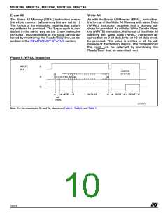
M93C86, M93C76, M93C66, M93C56, M93C46
INSTRUCTIONS
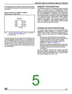
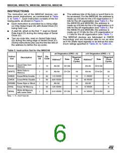
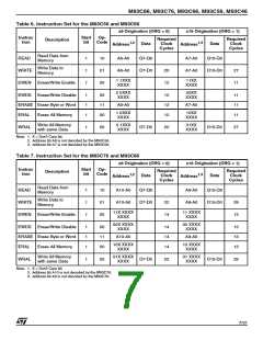
The instruction set of the M93Cx6 devices con-
tains seven instructions, as summarized in Table
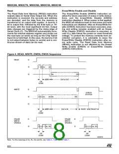
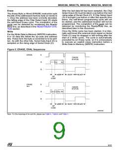
5. to Table 7.. Each instruction consists of the fol-
lowing parts, as shown in Figure 4.:
■
The address bits of the byte or word that is to
be accessed. For the M93C46, the address is
made up of 6 bits for the x16 organization or 7
bits for the x8 organization (see Table 5.). For
the M93C56 and M93C66, the address is
made up of 8 bits for the x16 organization or 9
bits for the x8 organization (see Table 6.). For
the M93C76 and M93C86, the address is
made up of 10 bits for the x16 organization or
11 bits for the x8 organization (see Table 7.).
■
■
■
Each instruction is preceded by a rising edge
on Chip Select Input (S) with Serial Clock (C)
being held Low.
A start bit, which is the first ‘1’ read on Serial
Data Input (D) during the rising edge of Serial
Clock (C).
Two op-code bits, read on Serial Data Input
(D) during the rising edge of Serial Clock (C).
(Some instructions also use the first two bits of
the address to define the op-code).
The M93Cx6 devices are fabricated in CMOS
technology and are therefore able to run as slow
as 0 Hz (static input signals) or as fast as the max-
imum ratings specified in Table 20. to Table 23..
Table 5. Instruction Set for the M93C46
x8 Origination (ORG = 0)
x16 Origination (ORG = 1)
Required
Instruc
tion
Start
bit
Op-
Code
Required
Clock
Description
1
1
Data
Data
Clock
Address
Address
Cycles
Cycles
Read Data from
Memory
READ
1
1
10
01
A6-A0
A6-A0
Q7-Q0
D7-D0
A5-A0
A5-A0
Q15-Q0
D15-D0
Write Data to
Memory
WRITE
18
25
EWEN Erase/Write Enable
EWDS Erase/Write Disable
ERASE Erase Byte or Word
1
1
1
1
00
00
11
00
11X XXXX
00X XXXX
A6-A0
10
10
10
10
11 XXXX
00 XXXX
A5-A0
9
9
9
9
ERAL
Erase All Memory
10X XXXX
10 XXXX
Write All Memory
with same Data
WRAL
1
00
01X XXXX D7-D0
18
01 XXXX
D15-D0
25
Note: 1. X = Don’t Care bit.
6/31

 STMICROELECTRONICS [ ST ]