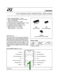
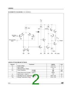
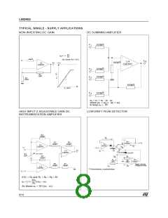
LM2902
ELECTRICAL CHARACTERISTICS (continued)
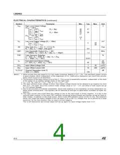
Symbol
Parameter
Min.
Typ.
Max.
Unit
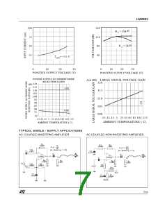
VOH
High Level Output Voltage
(VCC = +30V)
V
Tamb = +25oC
RL = 2kΩ
RL = 10kΩ
26
26
27
27
27
28
Tmin. ≤ Tamb ≤ Tmax
.
Tamb = +25oC
Tmin. ≤ Tamb ≤ Tmax
(VCC = +5V, RL = 2kΩ)
Tamb = +25oC
.
3.5
3
Tmin. ≤ Tamb ≤ Tmax
.
VOL
Low Level Output Voltage (RL = 10kΩ)
mV
Tamb = +25oC
5
20
20
Tmin. ≤ Tamb ≤ Tmax
.
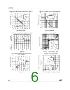
SR
Slew Rate (VCC = 15V, VI = 0.5 to 3V,
V/µs
MHz
%
RL = 2kΩ, CL = 100pF, unity gain)
0.4
1.3
GBP
THD
Gain Bandwidth Product (VCC = 30V
f = 100kHz, Vin = 10mV, RL = 2kΩ, CL = 100pF)
Total Harmonic Distortion
(f = 1kHz, AV = 20dB, RL = 2kΩ, VO = 2Vpp
CL = 100pF, VCC = 30V)
0.015
40
en
Equivalent Input Noise Voltage
(f = 1kHz, Rs = 100Ω, VCC = 30V)
nV
√Hz
DVio
DIIO
Input Offset Voltage Drift
Input Offset Current Drift
7
30
µV/oC
pA/oC
dB
10
200
VO1/VO2
Channel Separation (note 5)
1kHz ≤ f ≤ 20kHz
120
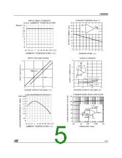
Notes : 1. Short-circuits from the output to VCC can cause excessive heating if VC C > 15V. The maximum output current
is approximately 40mA independent of the magnitude of VC C. Destructive di ssipation can result from simul ta-
neous short-circuit on all amplifiers.
2. The direction of the input current is out of the IC. This current is essentially constant, independent of the state
of the output so no loading change exists on the input lines.
+
+
3. Vo = 1.4V, Rs = 0Ω, 5V < VCC < 30V, 0 < Vic < VCC - 1.5V
4. The input common-mode voltage of either input signal voltage should not be allowed to go negative by more
+
than 0.3V. The upper end of the common-mode voltage range is VCC - 1.5V, but either or both inputs can go
to +32V without damage.
5. Due to the proximity of external components insure that coupling is not originating via stray capacitance be-
tween these external parts. This typically can be detected as this type of capacitance increases at higher fre-
quences.
6. This input current only exists when the voltage at any of the input leads is driven negative. It is due to the
collector-base junction of the input PNP transistor becoming forward biased and thereby acting as input di-
odes clamps. In addition to thi s diode action, there is also NPN parasitic action on the IC chip. this transistor
action can cause the output voltages of the Op-amps to go to the VCC voltage level (or to ground for a large
overdrive) for the time duration than an input is driven negative.
This is not destructive and normal output will set up again for input voltage higher than -0.3V.
4/14

 STMICROELECTRONICS [ ST ]