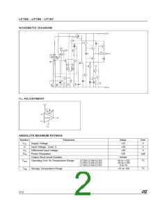
LF155 - LF156 - LF157
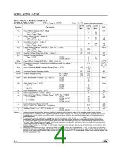
ELECTRICAL CHARACTERISTICS
LF355, LF356, LF357
0oC ≤ Tamb ≤ +70oC
VCC = ±15V, (unless otherwise specified)
LF355 - LF356 - LF357
Symbol
Parameter
Unit
Min.
Typ.
Max.
Vio
Input Offset Voltage (RS = 50Ω)
mV
Tamb = 25oC
3
10
13
Tmin. ≤ Tamb ≤ Tmax.
Iio
Input Offset Current - (note 3)
Tamb = 25oC
3
50
2
pA
nA
Tmin. ≤ Tamb ≤ Tmax.
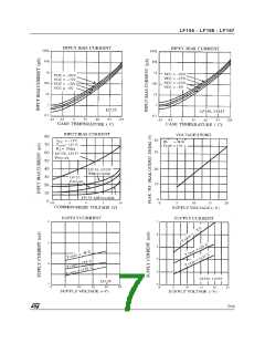
Iib
Input Bias Current - (note 3)
Tamb = 25oC
20
200
8
pA
nA
Tmin. ≤ Tamb ≤ Tmax.
Avd
Large Signal Voltage Gain (RL = 2kΩ, VO = ±10V)
V/mV
Tamb = 25oC
25
15
200
100
Tmin. ≤ Tamb ≤ Tmax.
SVR
ICC
Supply Voltage Rejection Ratio - (note 4)
Supply Current (no load)
80
dB
mA
Tamb = 25oC
LF355
2
5
4
10
LF356, LF357
DVio
Input Offset Voltage Drift (RS = 50Ω) - (note 2)
5
µV/oC
DVio/Vio Change in Average Temperature Coefficient with Vio adjust
0.5
µV/oC
(RS = 50Ω)
per mV
Vicm
Input Common Mode Voltage Range (Tamb = 25oC)
±10
+15.1
-12
V
CMR
Common Mode Rejection Ratio
80
100
dB
V
±VOPP
Output Voltage Swing
RL = 10kΩ
±12
±10
±13
±12
RL = 2kΩ
GBP
SR
Gain Bandwidth Product Tamb = 25oC)
LF355
LF356
LF357
2.5
5
20
MHz
Slew Rate (Tamb = 25oC)
AV = 1
V/µs
LF355
LF356
LF357
5
12
50
1012
3
AV = 5
Ri
Ci
en
Input Resistance (Tamb = 25oC)
Input Capacitance (Tamb = 25oC)
Ω
pF
Equivalent Input Noise Voltage (Tamb = 25oC, RS = 100Ω)
nV
√Hz
f = 1000Hz
LF355
20
12
25
15
LF356, LF357
LF355
f = 100Hz
LF356, LF357
in
ts
Equivalent Input Noise Current
pA
√Hz
µs
(Tamb = 25oC, f = 100Hz or f = 1000Hz)
0.01
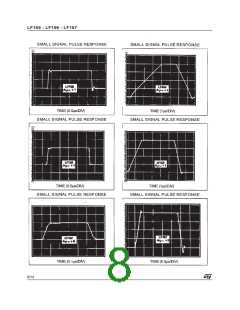
Settling Time (Tamb = 25oC) - (note 5)
LF355
LF356, LF357
4
1.5
Notes : 1. Unless otherwise specified the absolute maximum negative input voltage is equal to the negative power supply voltage.
2. The temperature coefficient of the adjusted input offset voltage changes only a small amount (0.5µV/oC typically) for each mV
of adjustment from its original unadjusted value. Common-mode rejection and open loop voltage gain are alsounaffected by
offset adjustment.
3. The input bias currents are junction leakage currents which approximately double for every 10oC increase in the junction
temperature Tamb. Due to limited production test time, the input bias current measured is correlated to junction temperature.
In a normal operation the junction temperature rises above the ambient temperature as a result of internal power dissipation,
Ptot-Tamb =Tamb +Rth(j-a)xPtot where Rth(j-a)is the thermal resistance from junction to ambient. Use of a heatsink is recommended
f input currents are to be kept to a minimum.
4. Supply voltage rejection is measured for both supply magnitudes increasing or decreasing simultaneously, in accordance with
common practise.
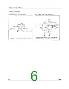
5. Settling time is defined here, for a unity gain inverter connection using 2kΩ resistors for the LF155, LF156 series. It is the time
required for the error voltage (the voltage at the inverting input pin on the amplifier) to settle to within 0.01% of its final value from
the time a 10V step input is applied to the inverter. For the LF157 series AV = -5, the feedback resistor from output to inputis 2kΩ
and the output step is 10V.
4/14

 STMICROELECTRONICS [ ST ]