L9613B
ELECTRICAL CHARACTERISTICS (continued)
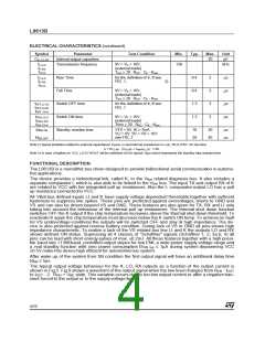
Symbol
Parameter
Test Condition
Min.
Typ.
Max.
Unit
pF
CKI,LO,RX
Internal output capacities
Transmission frequency
20
fLI-LO
fK-RX
fTX-K
9V < VS < 16V,
(external loads)
Tmin 20 R
130
kHz
CK - Kline
≥
KO
fLI-LO
fK-RX
fTX-K
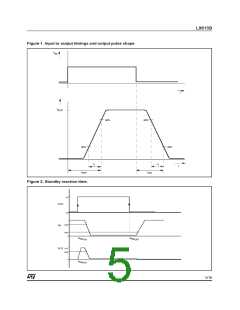
Rise Time
for the definition of tr, tf see
FIG. 1,
0.4
0.4
1.3
1.3
2
2
3
3
µs
2)
Fall Time
9V < VS < 16V,
(external loads)
s
s
µ
µ
Tmin 20 R
CK - Kline
≥
KO
tOFF,LI-LO
tOFF,K-RX
tOFF,TX-K
Switch OFF time
Switch ON time
Standby reaction time
for the definition of tr, tf see
FIG. 1
tON,LI-LO
tON,K-RX
tON,TX-K
9V < VS < 16V,
(external loads)
µs
Tmin 20 R
CK - Kline
≥
KO
tdSB ON
VTX = 0V, IK 7mA
10
20
20
40
s
s
≥
µ
µ
VLI = 0V, 9V < VS < 16V
see FIG. 2
tdSB OFF
Note 2) Speed limitation related to external capacitance CextRX, LO and internal impedance CLO,RX, RLO,RRX for rise time.
tr = RLO,RX (CLO,RX + CextRX, LO 1.38.
)
Note 3) In case of spikes on VCC 0.5V KOUT will be switched On for typical 10 s which represents the standby tdSB reaction time.
≥
µ
FUNCTIONAL DESCRIPTION
The L9613B is a monolithic bus driver designed to provide bidirectional serial communication in automo-
tive applications.
The device provides a bidirectional link, called K, to the VBat related diagnosis bus. It also includes a
separate comparator L which is also able to be linked to the VBat bus. The input TX and output RX of K
are related to VCC with her integrated pull up resistances. Also the L comparator output LO has a pull
up resistance connected to VCC.
All VBat bus defined inputs LI and K have supply voltage dependent thresholds together with sufficent
hysteresis to suppress line spikes. These pins are protected against overvoltages, shorts to GND and
VS and can also be driven beyond VS and GND. These features are also given for TX, RX and LI only
taking into account the behaviour of the internal pull up resistances. The thermal shut down function
switches OFF the K output if the chip temperature increases above the thermal shut down threshold. To
reactivate K again the chip temperature must decrease below the K switch ON temp. To achieve no fault
for VS undervoltage conditions the outputs will be switched OFF and stay at high impedance. The de-
vice is also protected against reverse battery condition. During lack of VS or GND all pins shows high
impedance characteristic. To realize a lack of the VS related bus line LI and K the outputs LO and RX
shows defined ON status. Supressing all 4 classes of ”Schaffner” signals (Schaffner 1; 2; 3a,b; 4) all
pins can be load with short energy pulses of max. ±0.2mJ. All these features together with a high possi-
ble baud rate >130Kbaud, controlled output slopes for low EMI, a wide power supply voltage range and
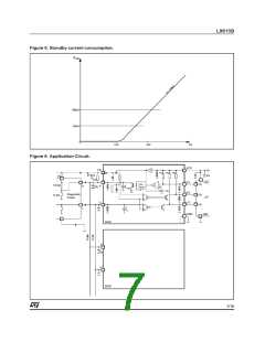
a real standby function with zero power consumption ISSB typ ≤ 1µA during system depowering VCC
≤0.5V make this device high efficient for automotivebus system.
After wake up of the system from SB condition the first output signal will have an additional delay time
tdtyp ≤ 5µs.
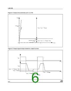
The typical output voltage behaviour for the K, LO, RX outputs as a function of the output current is
shown in Fig.5. Fig.6 shows a waveform of the output signal when the low level changes from RON IOUT
to IOUT 2 RON + UBE state. This variation occurs due to too low output current or after a negative tran-
sient forced to the output or to the supply voltage line.
4/10

 STMICROELECTRONICS [ ST ]