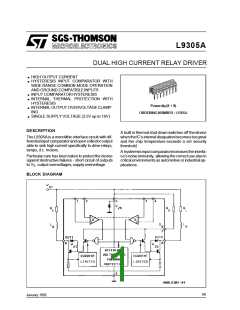
L9305A
ABSOLUTE MAXIMUM RATINGS
Symbol
Parameter
Value
(*) 20
26
Unit
V
V5
V7
IZS
Supply Voltage
Driver Supply Voltage
V
Supply Zener Clamp Current (DC)
(PULSED) (**)
30
80
mA
mA
VI
VI
Comparator Input Voltage Range
Differential Input Voltage
– 0.2 to 24
24
V
V
Tj, Tstg
Ptot
Junction and Storage Temperature
Power Dissipation at Tamb = 85°C
Output Current
– 55 to 150
928
°C
mW
Io
Int. limited
(*) The maximum allowed supply voltage without series resistors is limited by the built-in zener protection diodes
(**) Ton ≤ 2.5 ms ; repetition time ≥ 30 ms.
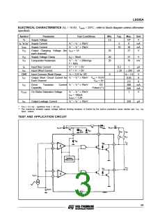
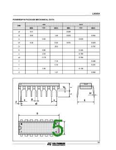
PIN CONNECTION (top view)
THERMAL DATA
Symbol
Rth j-pins
Rth j-amb
Parameter
Thermal Resistance Junction to pins
Thermal Resistance Junction to Ambient
Value
15
Unit
°C/W
°C/W
Max.
Max.
70
2/6

 STMICROELECTRONICS [ ST ]