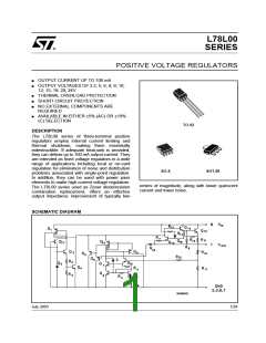
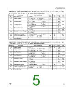
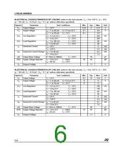
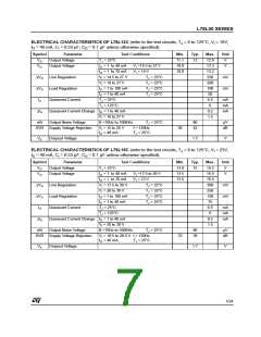
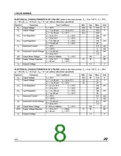
L78L00 SERIES
ABSOLUTE MAXIMUM RATINGS
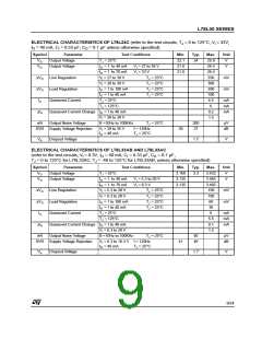
Symbol
Parameter²
Value
Unit
DC Input Voltage
V
V
V
= 3.3 to 9 V
30
O
O
O
V
= 12 to 15 V
= 18 to 24 V
35
V
I
40
100
I
Output Current
mA
O
P
T
Power Dissipation
Internally Limited (*)
tot
Storage Temperature Range
-40 to 150
0 to 125
°C
°C
stg
Operating Junction Temperature for L78L00C, L78L00AC
Range
T
op
for L78L00AB
-40 to 125
(*) Our SO-8 package used for Voltage Regulators is modified internally to have pins 2, 3, 6 and 7 electrically communed to the die attach
flag. This particular frame decreases the total thermal resistance of the package and increases its ability to dissipate power when an appro-
priate area of copper on the printed circuit board is available for heat-sinking. The external dimensions are the same as for the standard SO-8.
THERMAL DATA
Symbol
Parameter
SO-8
TO-92
SOT-89
Unit
R
Thermal Resistance Junction-case
Max
Max
20
15
°C/W
°C/W
thj-case
R
Thermal Resistance Junction-ambient
55 (*)
200
thj-amb
2
(*) Considering 6 cm of copper Board heat-sink
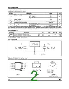
TEST CIRCUITS
CONNECTION DIAGRAM (top view)
PIN 1 = V
OUT
PIN 2 = GND
PIN 3 = V
IN
SO-8
SOT-89
TO-92
BOTTOM VIEW
2/24

 STMICROELECTRONICS [ ST ]