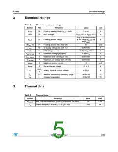
L6699
Electrical data
5
Electrical data
Tj = -25 to +125 °C, VCC = 15 V, VBOOT = 15 V, CHVG = CLVG = 1 nF; CF = 470 pF;
RFmin = 12 KΩ; unless otherwise specified.
Table 5.
Symbol
Electrical characteristics
Parameter
Test condition
Min.
Typ.
Max.
Unit
Ic supply voltage
VCC
VCCOn
VCCOff
Hys
Operating range
Turn-on threshold
After device turn-on
8.85
10
16
V
V
V
V
V
Voltage rising
Voltage falling
10.7
8.15
2.55
17
11.4
8.85
Turn-off threshold
Hysteresis
7.45
VZ
VCC clamp voltage
Iclamp = 15 mA
16
17.9
Supply current
Before device turn-on
Istart-up
Startup current
250
300
µA
VCC = VCCOn - 0.2 V
Iq
Quiescent current
Operating current
Device on, VSTBY = 1 V
1
3
1.3
4.1
mA
mA
Iop
Device on, VSTBY = VRFmin
VDIS>1.92 V or VDELAY>3.65 V or
VLINE<1.2 V
Iq
Residual consumption
400
500
µA
High-side floating gate-drive supply
Synchronous bootstrap diode
ON-resistance
RDS(on)
VLVG = high
150
Overcurrent comparator
IISEN
Input bias current
VISEN = 0 to VISENdis
Voltage rising (1)
Voltage rising (1)
-1
µA
V
VISENx
Frequency shift threshold
0.76
1.43
0.80
1.5
0.84
1.55
VISENdis Immediate stop threshold
V
Line sensing
VLINE
IHys
Threshold voltage
Current hysteresis
Clamp level
Voltage rising or falling (1)
VLINE = 1.2 V
1.18
10
6
1.22
13
1.26
16
V
µA
V
Vclamp
ILINE = 1 mA
Latched disable function
IDIS
VDIS
Input bias current
Disable threshold
VDIS = 0 to 1.92 V
Voltage rising (1)
-1
µA
V
1.78
1.85
1.92
Oscillator
58.2
225
60
61.8
245
fosc
Oscillation frequency
kHz
RRFmin = 2.7 kΩ
235
Doc ID 022835 Rev 2
9/38

 STMICROELECTRONICS [ ST ]