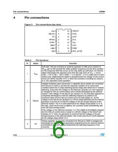
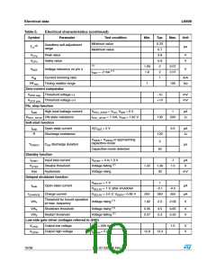
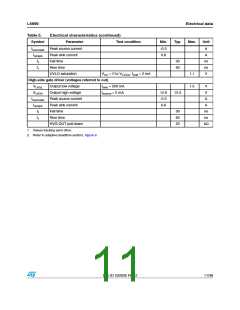
Pin connections
Table 4.
L6699
Pin functions (continued)
N.
Name
Function
Chip ground. Current return for both the low-side gate-drive current and the
bias current of the IC. All of the ground connections of the bias components
should be tied to a track going to this pin and kept separate from any pulsed
current return.
10
GND
Low-side gate-drive output. The driver is capable of 0.3 A min. source and 0.8 A
min. sink peak current to drive the lower MOSFET of the half bridge leg. The pin
is actively pulled to GND during UVLO.
11
12
13
14
LVG
VCC
N.C.
OUT
Supply voltage of both the signal part of the IC and the low-side gate driver.
Sometimes a small bypass capacitor (0.1 µF typ.) to GND may be useful to
obtain a clean bias voltage for the signal part of the IC.
High voltage spacer. The pin is not internally connected to isolate the high
voltage pin and ease compliance with safety regulations (creepage distance) on
the PCB.
High-side gate-drive floating ground. Current return for the high-side gate-drive
current. Lay out the connection of this pin carefully to avoid too large spikes
below ground.
High-side floating gate-drive output. The driver is capable of 0.3 A min. source
and 0.8 A min. sink peak current to drive the upper MOSFET of the half bridge
leg. A resistor internally connected to pin 14 (OUT) ensures that the pin is not
floating during UVLO.
15
HVG
High-side gate-drive floating supply voltage. The bootstrap capacitor connected
between this pin and pin 14 (OUT) is fed by an internal synchronous bootstrap
diode driven in-phase with the low-side gate-drive. This patented structure
replaces the normally used external diode.
16
VBOOT
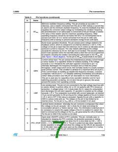
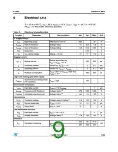
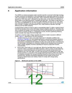
Figure 3.
Typical system block diagram
0&# 02%
ꢇ
2%'5,!4/2 ꢈ/04)/.!,ꢉ
2%3/.!.4 (!,&ꢇ"2)$'%
OUTDC
6
(!,&
ꢇ"2)$'%
INAC
6
-)$0/).4
2ESON ANT (" IS TURN ED O FF IN CASE O F
0&#gS ANO MALOUSOPERATIONꢅ FORSAFETY
,ꢁꢄꢁꢊ!ꢅ,ꢁꢄꢁꢂ
3ꢎ(
,ꢁꢄꢁꢋꢅ,ꢁꢄꢁꢋ
,ꢋꢌꢍꢋ
4ꢎ(
,ꢁꢁꢌꢌ
0&# CAN BE TURNED OFF AT LIGH T
LO AD TO EASE CO MPLIANCE WITH
ENERGY SAVING REGULATIONSꢆ
!-ꢀꢀꢂꢃꢃVꢀ
8/38
Doc ID 022835 Rev 2

 STMICROELECTRONICS [ ST ]