L6699
Application information
6.1
Oscillator
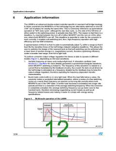
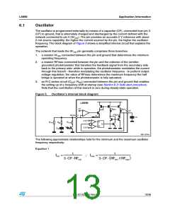
The oscillator is programmed externally by means of a capacitor (CF), connected from pin 3
(CF) to ground, that is alternately charged and discharged by the current defined with the
network connected to pin 4 (RFmin). The pin provides an accurate 2 V reference with about
2 mA source capability; the higher the current sourced by the pin, the higher the oscillator
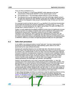
frequency. The block diagram of Figure 5 shows a simplified internal circuit that explains the
operation.
The network that loads the RFmin pin generally comprises three branches:
1. a resistor RFmin connected between the pin and ground that determines the minimum
operating frequency.
2. a resistor RFmax connected between the pin and the collector of the (emitter-
grounded) phototransistor that transfers the feedback signal from the secondary side
back to the primary side; while in operation, the phototransistor modulates the current
through this branch - therefore modulating the oscillator frequency - to perform output
voltage regulation; the value of RFmax determines the maximum frequency the half
bridge is operated at when the phototransistor is fully saturated.
3. an R-C series circuit (CSS+ RSS) connected between the pin and ground that enables
the setting up of a frequency shift at startup (see Section 6.3: Safe-start procedure).
Note that the contribution of this branch is zero during steady-state operation.
Figure 5.
Oscillator's internal block diagram
,ꢁꢁꢌꢌ
ꢊ 6
ꢏ
+-q)2
+-q)2
ꢂ
#&
ꢊq+-q)2
ꢇ
2&MIN
ꢋ
)
2
#&
ꢏ
ꢇ
ꢐꢆꢌ 6
3
2
2&MIN
2&MAX
233
1
ꢏ
ꢇ
ꢂꢆꢌ 6
#
33
!-ꢀꢀꢂꢃꢌVꢀ
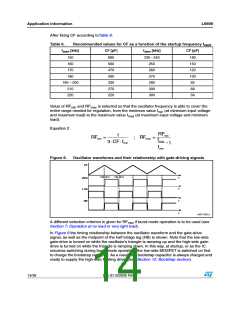
The following approximate relationships hold for the minimum and the maximum oscillator
frequency respectively:
Equation 1
1
1
fmin
=
; fmax =
(
)
3·CF·RFmin
3·CF · RFmin // RFmax
Doc ID 022835 Rev 2
13/38

 STMICROELECTRONICS [ ST ]