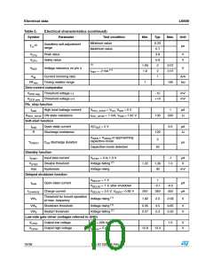
Electrical data
L6699
Table 5.
Symbol
Electrical characteristics (continued)
Parameter
Test condition
Minimum value
Min.
Typ.
Max.
Unit
0.23
0.7
3.9
0.9
2
Deadtime self-adjustment
range
(2)
TD
µs
Maximum value
VCFp
VCFv
Peak value
Valley value
V
V
(1)
1.93
1.8
2.07
2.07
VREF
Voltage reference on pin 4
V
IREF = -2 mA (1)
2
KM
Current mirroring ratio
Timing resistor range
1
A/A
RFmin
1
100
kΩ
Zero-current comparator
VZCD neg Threshold voltage (-)
VZCD pos Threshold voltage (+)
Pfc_stop function
-10
mV
mV
+10
Ileak
High level leakage current
VPFC_STOP = VCC, VDIS = 0 V
1
µA
RPFC_STOP ON-state resistance
IPFC_STOP = 1 mA, VDIS > 1.92 V
130
200
Ω
Soft-start function
Ileak
R
Open-state current
V(CSS) = 2 V
0.5
µA
Discharge resistance
120
5
Ω
VISEN > VISENx or approaching
capacitive-mode
TDISCH
CSS discharge duration
µs
Capacitive-mode detected
50
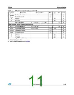
Standby function
ISTBY
VSTBY
Hys
Input bias current
VSTBY = 0 to 1.3 V
Voltage falling (1)
Voltage rising
-1
µA
V
Disable threshold
Hysteresis
1.22
1.26
30
1.3
mV
Delayed shutdown function
Ileak Open-state current
ICHARGE Charge current
V
DELAY = 1 V
1
µA
VDELAY = 1 V, after shutdown
VDELAY = 2.5 V, VISEN = 0.85 V
-0.1
350
-0.5
450
250
µA
V
Threshold for forced operation
Vth1
Voltage rising (1)
1.92
2.0
2.08
at max. frequency
Shutdown threshold
Restart threshold
Vth2
Vth3
Voltage rising (1)
Voltage falling (1)
3.35
0.27
3.5
0.3
3.65
0.33
V
V
Low-side gate driver (voltages referred to GND)
VLVGL
VLVGH
Output low voltage
Output high voltage
Isink = 200 mA
Isource = 5 mA
1.5
V
V
12.8
13.3
10/38
Doc ID 022835 Rev 2

 STMICROELECTRONICS [ ST ]