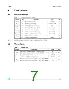
Electrical characteristics
L6599
5
Electrical characteristics
T = 0 to 105 °C, V = 15 V, V
= 15 V, C
= C
= 1 nF; C = 470 pF;
LVG F
J
CC
BOOT
HVG
R
= 12 kΩ; unless otherwise specified.
RFmin
Table 5.
Symbol
Electrical characteristics
Parameter
Test condition
Min
Typ
Max
Unit
IC supply voltage
VCC
Operating range
After device turn-on
Voltage rising
8.85
10
16
V
V
V
V
V
VCC(ON)
VCC(OFF)
Turn-ON threshold
10.7
8.15
2.55
17
11.4
8.85
Turn-OFF threshold
Hysteresis
Voltage falling
7.45
Hys
VZ
VCC clamp voltage
Iclamp = 10 mA
16
17.9
Supply current
Istart-up
Iq
Before device turn-ON
VCC = VCC(ON) - 0.2 V
Start-up current
Quiescent current
Operating current
200
1.5
3.5
250
2
µA
mA
mA
Device ON, VSTBY = 1 V
Device ON,
VSTBY = VRFmin
Iop
5
VDIS > 1.85 V or VDELAY
Iq
Residual consumption
300
400
µA
> 3.5 V or VLINE < 1.25 V
or VLINE = Vclamp
High-side floating gate-drive supply
VBOOT pin leakage
ILKBOOT
5
5
µA
µA
Ω
VBOOT = 580 V
VOUT = 562 V
current
ILKOUT
rDS(on)
OUT pin leakage current
Synchronous bootstrap
diode ON-resistance
150
VLVG = High
Overcurrent comparator
IISEN
tLEB
VISEN = 0 to VISENdis
Input bias current
-1
µA
ns
After VHVG and VLVG
low-to-high transition
Leading edge blanking
250
0.8
Frequency shift
threshold
Voltage rising (1)
VISENx
0.76
1.44
0.84
V
Hysteresis
Voltage falling
50
1.5
300
mV
V
Voltage rising (1)
VISENdis
td(H-L)
Latch OFF threshold
Delay to output
1.56
400
ns
8/36

 STMICROELECTRONICS [ ST ]