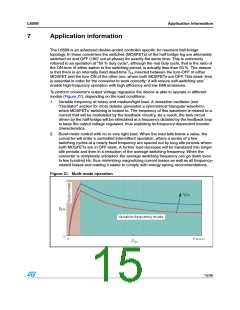
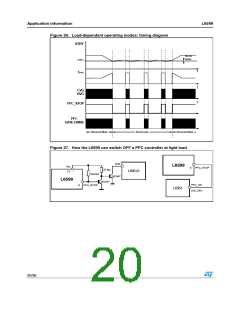
Application information
L6599
7.1
Oscillator
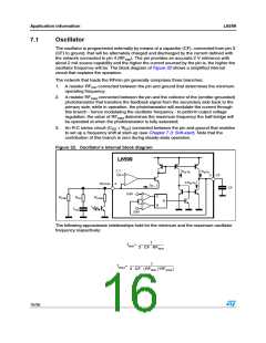
The oscillator is programmed externally by means of a capacitor (CF), connected from pin 3
(CF) to ground, that will be alternately charged and discharged by the current defined with
the network connected to pin 4 (RF ). The pin provides an accurate 2 V reference with
min
about 2 mA source capability and the higher the current sourced by the pin is, the higher the
oscillator frequency will be. The block diagram of Figure 22 shows a simplified internal
circuit that explains the operation.
The network that loads the RFmin pin generally comprises three branches:
1. A resistor RF
connected between the pin and ground that determines the minimum
min
operating frequency;
2. A resistor RF
connected between the pin and the collector of the (emitter-grounded)
max
phototransistor that transfers the feedback signal from the secondary side back to the
primary side; while in operation, the phototransistor will modulate the current through
this branch - hence modulating the oscillator frequency - to perform output voltage
regulation; the value of RF
determines the maximum frequency the half-bridge will
max
be operated at when the phototransistor is fully saturated;
3. An R-C series circuit (C + R ) connected between the pin and ground that enables
SS
SS
to set up a frequency shift at start-up (see Chapter 7.3: Soft-start). Note that the
contribution of this branch is zero during steady-state operation.
Figure 22. Oscillator's internal block diagram
L6599
2 V
KM·IR
KM·IR
+
-
3
CF
2·KM·IR
RFmin
4
IR
CF
0.9V
1 V
+
-
S
R
RFmin
RSS
RFmax
Q
+
-
CSS
3.9V
4 V
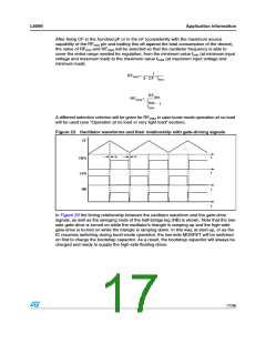
The following approximate relationships hold for the minimum and the maximum oscillator
frequency respectively:
1
f
min= ------------------------------------
3 ⋅ CF ⋅ RFmin
1
f
max= -----------------------------------------------------------------
||
3 ⋅ CF ⋅ (RFmin RFmax
)
16/36

 STMICROELECTRONICS [ ST ]