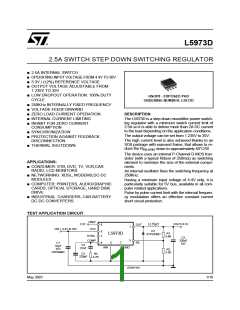
L5973D
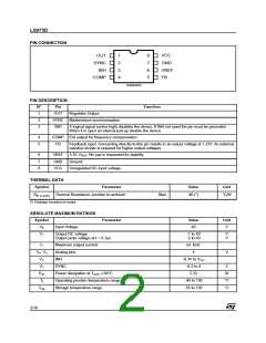
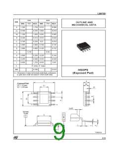
PIN CONNECTION
VCC
GND
VREF
FB
OUT
SYNC
INH
1
2
3
4
8
7
6
5
COMP
D98IN955
PIN DESCRIPTION
N°
1
Pin
Function
OUT
Regulator Output.
2
SYNC Master/slave synchronization.
3
INH
A logical signal (active high) disables the device. If INH not used the pin must be grounded.
When it is open an internal pull-up disable the device.
4
5
COMP E/A output for frequency compensation.
FB
Feedback input. Connecting directly to this pin results in an output voltage of 1.23V. An external
resistive divider is required for higher output voltages.
6
7
8
VREF
GND
VCC
3.3V V . No cap is requested for stability.
REF
Ground.
Unregulated DC input voltage.
THERMAL DATA
Symbol
Parameter
Value
Unit
R
Thermal Resistance Junction to ambient
Max.
40 (*)
°C/W
th (j-amb)
(*) Package mounted on board
ABSOLUTE MAXIMUM RATINGS
Symbol
Parameter
Value
Unit
V
Input Voltage
40
V
8
1
V
Output DC voltage
Output peak voltage at t = 0.1µs
-1 to 40
-5 to 40
V
V
I
Maximum output current
int. limit.
4
1
V , V
4
Analog pins
INH
V
5
V
-0.3V to V
CC
3
2
V
SYNC
-0.3 to 4
2.25
V
P
Power dissipation at T
≤ 60°C
W
°C
°C
tot
amb
T
Operating junction temperature range
Storage temperature range
-40 to 150
-55 to 150
j
T
stg
2/10

 STMICROELECTRONICS [ ST ]