L4805-L4808-L4885-L4892-L4810-L4812
ABSOLUTE MAXIMUM RATINGS
Symbol
Parameter
Value
+ 35
- 18
60
Unit
V
VI
DC Input Voltage
DC Input Reverse Voltage
V
Transient Input Overvoltages :
Load Dump :
V
5ms < Trise < 10ms,
τf Fall Time Constant = 100ms,
Rsource < 0.5Ω
Field Decay :
- 60
V
5ms < tfall < 10ms, Rsource < 10Ω
τr Rise Time Constant = 33ms
Junction and Storage Temperature Range
Tj, Tstg
- 55 to + 150
°C
THERMAL DATA
Symbol
Parameter
SOT82
TO220
Unit
Rth j-case
Rth j-amb
Thermal Resistance Junction-case
Max.
Max.
8
4
°C/W
°C/W
Thermal Resistance Junction-ambient
100
75
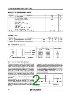
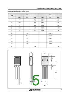
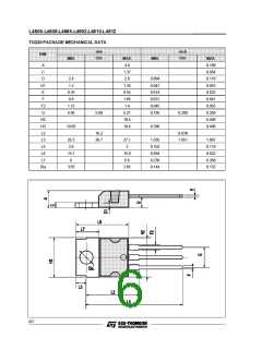
PIN CONNECTION (top view)
Order Codes
Output Voltage
TO-220
SOT-82
L4805CV
L4808CV
L4885CV
L4892CV
L4810CV
L4812CV
L4805CX
L4808CX
L4885CX
L4892CX
L4810CX
L4812CX
5V
8V
8.5 V
9.2 V
10 V
12 V
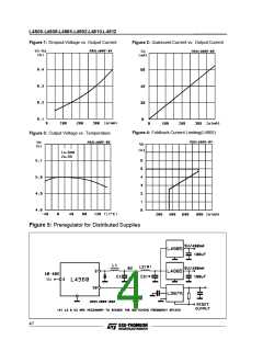
TEST AND APPLICATION CIRCUIT
Theoutput capacitorisrequired forstability. Though
the 100 µF shown is the minimum recommended
value, actual size and type may vary depending
upon the application load and temperature range.
Capacitoreffectiveseriesresistance (ESR)alsofac-
tors in the IC stability. Since ESR varies from one
brandtothe next,some bench workmay be required
to determine the minimum capacitor value to use in
production. Worst-case is usuallydetermined at the
minimum ambient temperature and maximum load
expected.
Capacitorsmust also berated at all ambient tempe-
ratureexpectedin the system. Many aluminum type
electrolyticswill freeze at temperatures less than –
30 °C, reducing their effective capacitance to zero.
To maintain regulatorstability down to – 40 °C, ca-
pacitors rated at that temperature (such as tan-
talums) must be used.
Output capacitors can be increased in size to any
desired value above the minimum. One possible
purpose of this would be to maintain the output vol-
tages during brief conditions of negative input tran-
sients that might be characteristics of a particular
system.
2/7

 STMICROELECTRONICS [ ST ]