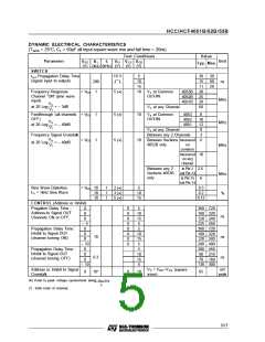
HCC/HCF4051B/52B/53B
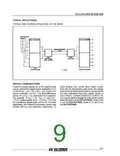
TYPICAL APPLICATIONS
TYPICAL TIME-DIVISION APPLICATION OF THE 4052B
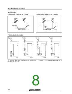
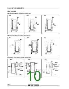
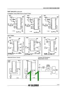
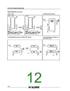
SPECIAL CONSIDERATIONS
Control of analog signals up to 20V peak-to-peak
can be achieved by digital signal amplitudes of 4.5
to 20V(if VDD – VSS = 3V, a VDD – VEE of up to 13V
can be controlled ; for VDD – VEE level differences
above 13V, a VDD – VSS ofat least 4.5V is required).
avoid drawing VDD current when switch current
flows into the transmission gate inputs, the voltage
drop across the bidirectional switch mustnot exceed
0,8 volt (valvulated from RON values shown in
ELECTRICAL CHARACTERISTICS CHART). No
VDD current will flow through RL if the switch current
flows into lead3 on the HCC/HCF4051 ; leads 3 and
13 on the HCC/HCF4052 ; leads 4, 14, and 15 on
the HCC/HCF4053.
For example, if VDD = + 5V, VSS = 0, and VEE
=
–13.5V, analog signals from – 13.5V to + 4.5V can
be controlled by digital inputs of 0 to 4.5V. In certain
applications, the external load-resistor current may
include both VDD and signal-line components. To
9/17

 STMICROELECTRONICS [ ST ]