ST3M01
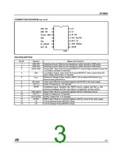
CONNECTION DIAGRAM (top view)
PIN DESCRIPTION
Pin N°
Symbol
Name and Function
1
2
3
GND SW
GND SW
Switching Ground. Must be low impedance; solder directly to GND plane
Switching Ground. Must be low impedance; solder directly to GND plane
Virtual GND
Virtual GND. Open Drain N-Cnannel MOSFET: must be high impedance when the
Low Battery condition is detected.
4
5
LBO
Low Battery Output. Open Drain N-Cnannel MOSFET: sinks current when the
input voltage drops below 2V typically.
V
Reference Voltage Output. Bypass with 0.1 µF to improve the linears V
REF
REF
thermal noise performance.
6
7
IN Linear
OUT L
Linear Input. Must be connected togheter with IN SW to the input supply.
Linear B Output port. 1.9V typically.
B
8
SHDN
Shutdown Input. Disables the SMPS and L output, but the L , the
A
B
referencevoltage and the low batery comparator remain active.
Signal GND. Must be connected togheter with the Switching Ground.
Linear A Output port. 3V typically.
9
GND Signal
10
OUT L
A
11
12
13
14
OUT DC/DC
DC/DC Output Port: 3.3V typically.
IN SW
LX
SMPS Input. Must be connected togheter with IN_Linear to the input supply.
1.5A N-Channel Power MOSFET Drain.
LX
1.5A N-Channel Power MOSFET Drain.
3/11

 STMICROELECTRONICS [ ST ]