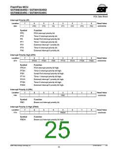
FlashFlex MCU
SST89E564RD / SST89V564RD
SST89E554RC / SST89V554RC
EOL Data Sheet
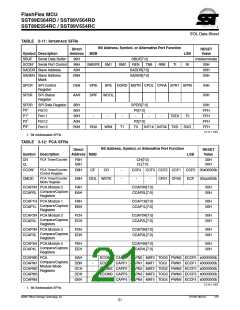
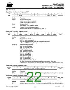
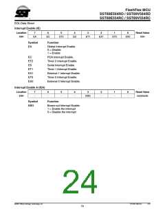
SuperFlash Configuration Register (SFCF)
Location
7
6
5
4
3
2
1
0
Reset Value
B1H
-
IAPEN
-
-
-
-
SWR
BSEL
x0xxxx00b
Symbol
Function
Enable IAP operation
IAPEN
0: IAP commands are disabled
1: IAP commands are enabled
SWR
BSEL
Software Reset
See Section 10.2, “Software Reset”
Program memory block switching bit
See Figure 3-1, Figure 3-2, Table 3-3, and Table 3-4.
SuperFlash Command Register (SFCM)
Location
7
6
5
4
3
2
1
0
Reset Value
B2H
FIE
FCM6
FCM5
FCM4
FCM3
FCM2
FCM1
FCM0
00H
Symbol
Function
FIE
Flash Interrupt Enable.
0: INT1# is not reassigned.
1: INT1# is re-assigned to signal IAP operation completion.
External INT1# interrupts are ignored.
FCM[6:0]
Flash operation command
000_0001b Chip-Erase
000_1011b Sector-Erase
000_1101b Block-Erase
000_1100b Byte-Verify1
000_1110b Byte-Program
000_1111b Prog-SB1
000_0011b Prog-SB2
000_0101b Prog-SB3
000_1001b Prog-SC0
000_1001b Prog-SC1
000_1000bEnable-Clock-Double
All other combinations are not implemented, and reserved for future use.
1. Byte-Verify has a single machine cycle latency and will not generate any INT1# interrupt regardless of FIE.
SuperFlash Address Registers (SFAL)
Location
7
6
5
4
3
2
1
0
Reset Value
B3H
SuperFlash Low Order Byte Address Register
00H
Symbol
Function
Mailbox register for interfacing with flash memory block. (Low order address register).
SFAL
SuperFlash Address Registers (SFAH)
Location
7
6
5
4
3
2
1
0
Reset Value
B4H
SuperFlash High Order Byte Address Register
00H
Symbol
Function
Mailbox register for interfacing with flash memory block. (High order address register).
SFAH
©2007 Silicon Storage Technology, Inc.
S71207-08-EOL
1/07
22

 SST [ SILICON STORAGE TECHNOLOGY, INC ]