4 Mbit SPI Serial Flash
SST25VF040B
Data Sheet
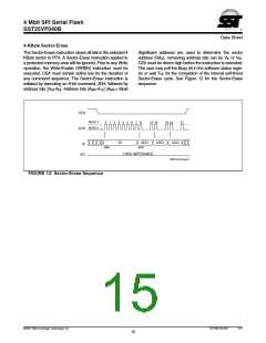
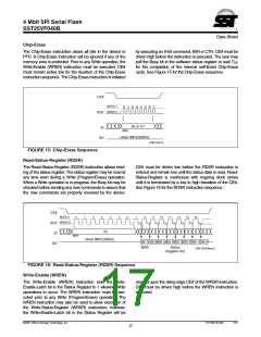
Chip-Erase
The Chip-Erase instruction clears all bits in the device to
FFH. A Chip-Erase instruction will be ignored if any of the
memory area is protected. Prior to any Write operation, the
Write-Enable (WREN) instruction must be executed. CE#
must remain active low for the duration of the Chip-Erase
instruction sequence. The Chip-Erase instruction is initiated
by executing an 8-bit command, 60H or C7H. CE# must be
driven high before the instruction is executed. The user may
poll the Busy bit in the software status register or wait TCE
for the completion of the internal self-timed Chip-Erase
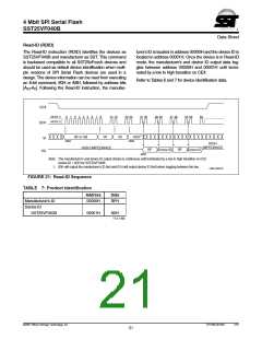
cycle. See Figure 15 for the Chip-Erase sequence.
CE#
MODE 3
0
1
2
3
4
5
6
7
MODE 0
SCK
60 or C7
SI
MSB
HIGH IMPEDANCE
SO
1295 ChEr.0
FIGURE 15: Chip-Erase Sequence
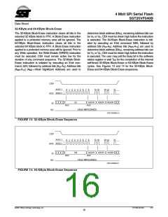
Read-Status-Register (RDSR)
The Read-Status-Register (RDSR) instruction allows read-
ing of the status register. The status register may be read at
any time even during a Write (Program/Erase) operation.
When a Write operation is in progress, the Busy bit may be
checked before sending any new commands to assure that
the new commands are properly received by the device.
CE# must be driven low before the RDSR instruction is
entered and remain low until the status data is read. Read-
Status-Register is continuous with ongoing clock cycles
until it is terminated by a low to high transition of the CE#.
See Figure 16 for the RDSR instruction sequence.
CE#
MODE 3
MODE 0
0
1
2
3
4
5
6
7
8
9
10
11
12
13
14
SCK
SI
05
HIGH IMPEDANCE
MSB
Bit 7 Bit 6 Bit 5 Bit 4 Bit 3 Bit 2 Bit 1 Bit 0
SO
MSB
Status
1295 RDSRseq.0
Register Out
FIGURE 16: Read-Status-Register (RDSR) Sequence
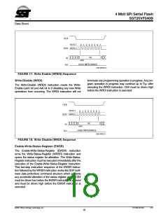
Write-Enable (WREN)
The Write-Enable (WREN) instruction sets the Write-
Enable-Latch bit in the Status Register to 1 allowing Write
operations to occur. The WREN instruction must be exe-
cuted prior to any Write (Program/Erase) operation. The
WREN instruction may also be used to allow execution of
the Write-Status-Register (WRSR) instruction; however,
the Write-Enable-Latch bit in the Status Register will be
cleared upon the rising edge CE# of the WRSR instruction.
CE# must be driven high before the WREN instruction is
executed.
©2007 Silicon Storage Technology, Inc.
S71295-02-000
7/07
17

 SST [ SILICON STORAGE TECHNOLOGY, INC ]