A d v a n c e I n f o r m a t i o n
Any commands written during the chip erase operation are ignored, including
erase suspend commands. However, note that a hardware reset immediately
terminates the erase operation. If that occurs, the chip erase command sequence
should be reinitiated once the device has returned to reading array data, to en-
sure data integrity.
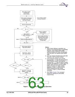
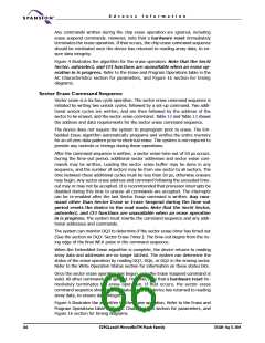
Figure 4 illustrates the algorithm for the erase operation. Note that the SecSi
Sector, autoselect, and CFI functions are unavailable when an erase op-
eration in is progress. Refer to the Erase and Program Operations table in the
AC Characteristics section for parameters, and Figure 16 section for timing
diagrams.
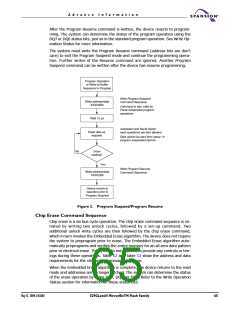
Sector Erase Command Sequence
Sector erase is a six bus cycle operation. The sector erase command sequence is
initiated by writing two unlock cycles, followed by a set-up command. Two addi-
tional unlock cycles are written, and are then followed by the address of the
sector to be erased, and the sector erase command. Table 12 and Table 13 shows
the address and data requirements for the sector erase command sequence.
The device does not require the system to preprogram prior to erase. The Em-
bedded Erase algorithm automatically programs and verifies the entire memory
for an all zero data pattern prior to electrical erase. The system is not required to
provide any controls or timings during these operations.
After the command sequence is written, a sector erase time-out of 50 µs occurs.
During the time-out period, additional sector addresses and sector erase com-
mands may be written. Loading the sector erase buffer may be done in any
sequence, and the number of sectors may be from one sector to all sectors. The
time between these additional cycles must be less than 50 µs, otherwise erasure
may begin. Any sector erase address and command following the exceeded time-
out may or may not be accepted. It is recommended that processor interrupts be
disabled during this time to ensure all commands are accepted. The interrupts
can be re-enabled after the last Sector Erase command is written. Any com-
mand other than Sector Erase or Erase Suspend during the time-out
period resets the device to the read mode. Note that the SecSi Sector,
autoselect, and CFI functions are unavailable when an erase operation
in is progress. The system must rewrite the command sequence and any addi-
tional addresses and commands.
The system can monitor DQ3 to determine if the sector erase timer has timed out
(See the section on DQ3: Sector Erase Timer.). The time-out begins from the ris-
ing edge of the final WE# pulse in the command sequence.
When the Embedded Erase algorithm is complete, the device returns to reading
array data and addresses are no longer latched. The system can determine the
status of the erase operation by reading DQ7, DQ6, or DQ2 in the erasing sector.
Refer to the Write Operation Status section for information on these status bits.
Once the sector erase operation has begun, only the Erase Suspend command is
valid. All other commands are ignored. However, note that a hardware reset im-
mediately terminates the erase operation. If that occurs, the sector erase
command sequence should be reinitiated once the device has returned to reading
array data, to ensure data integrity.
Figure 4 illustrates the algorithm for the erase operation. Refer to the Erase and
Program Operations table in the AC Characteristics section for parameters, and
Figure 16 section for timing diagrams.
66
S29GLxxxN MirrorBitTM Flash Family
27631A4 May 13, 2004

 SPANSION [ SPANSION ]