A d v a n c e I n f o r m a t i o n
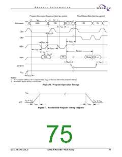
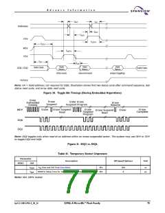
tAHT
tAS
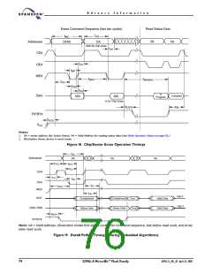
Addresses
CE#
tAHT
tASO
tCEPH
tOEH
WE#
OE#
tOEPH
tDH
Valid Data
tOE
Valid
Status
Valid
Status
Valid
Status
DQ6 / DQ2
Valid Data
(first read)
(second read)
(stops toggling)
RY/BY#
Note: VA = Valid address; not required for DQ6. Illustration shows first two status cycle after command sequence, last
status read cycle, and array data read cycle.
Figure 20. Toggle Bit Timings (During Embedded Algorithms)
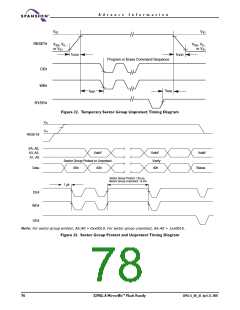
Enter
Embedded
Erasing
Erase
Suspend
Enter Erase
Suspend Program
Erase
Resume
Erase
Erase Suspend
Read
Erase
Suspend
Program
Erase
Complete
WE#
Erase
Erase Suspend
Read
DQ6
DQ2
Note: DQ2 toggles only when read at an address within an erase-suspended sector. The system may use OE# or CE#
to toggle DQ2 and DQ6.
Figure 21. DQ2 vs. DQ6
Table 41. Temporary Sector Unprotect
Parameter
Description
All Speed Options
Unit
JEDEC
Std
t
V
Rise and Fall Time (See Note)
Min
Min
500
4
ns
µs
VIDR
ID
t
RESET# Setup Time for Temporary Sector Unprotect
RSP
Note: Not 100% tested.
April 22, 2005 S29GL-A_00_A3
S29GL-A MirrorBit™ Flash Family
75

 SPANSION [ SPANSION ]