A d v a n c e I n f o r m a t i o n
all internal program/erase circuits are disabled, and the device resets to the read
mode. Subsequent writes are ignored until V is greater than V
. The system
LKO
CC
must provide the proper signals to the control pins to prevent unintentional
writes when V is greater than V
.
LKO
CC
Write Pulse Glitch Protection
Noise pulses of less than 3 ns (typical) on OE#, CE# or WE# do not initiate a
write cycle.
Logical Inhibit
Write cycles are inhibited by holding any one of OE# = V , CE# = V or WE#
IL
IH
= V . To initiate a write cycle, CE# and WE# must be a logical zero while OE#
IH
is a logical one.
Power-Up Write Inhibit
If WE# = CE# = V and OE# = V during power up, the device does not accept
IL
IH
commands on the rising edge of WE#. The internal state machine is automati-
cally reset to the read mode on power-up.
Common Flash Memory Interface (CFI)
The Common Flash Interface (CFI) specification outlines device and host system
software interrogation handshake, which allows specific vendor-specified soft-
ware algorithms to be used for entire families of devices. Software support can
then be device-independent, JEDEC ID-independent, and forward- and back-
ward-compatible for the specified flash device families. Flash vendors can
standardize their existing interfaces for long-term compatibility.
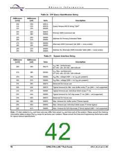
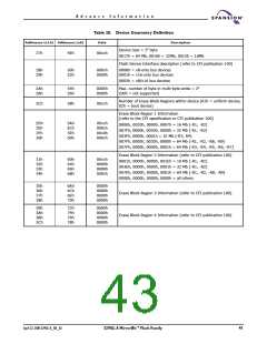
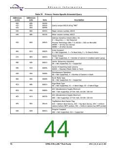
This device enters the CFI Query mode when the system writes the CFI Query
command, 98h, to address 55h, any time the device is ready to read array data.
The system can read CFI information at the addresses given in Tables 26–29. To
terminate reading CFI data, the system must write the reset command.
The system can also write the CFI query command when the device is in the au-
toselect mode. The device enters the CFI query mode, and the system can read
CFI data at the addresses given in Tables 26–29. The system must write the
reset command to return the device to reading array data.
For further information, please refer to the CFI Specification and CFI Publication
100. Alternatively, contact your sales representative for copies of these
documents.
April 22, 2005 S29GL-A_00_A3
S29GL-A MirrorBit™ Flash Family
39

 SPANSION [ SPANSION ]