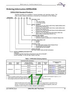
A d v a n c e I n f o r m a t i o n
Pin Descriptions
A21–A0
=
=
=
=
=
=
22 Address inputs
21 Address inputs
20 Address inputs
8 Data inputs/outputs
15 Data inputs/outputs
DQ15 (Data input/output, word mode), A-1 (LSB
Address input, byte mode)
Chip Enable input
Output Enable input
Write Enable input
A20–A0
A19–A0
DQ7–DQ0
DQ14–DQ0
DQ15/A-1
CE#
OE#
WE#
WP#/ACC
=
=
=
=
Hardware Write Protect input/Programming
Acceleration input
ACC
WP#
RESET#
RY/BY#
BYTE#
=
=
=
=
=
=
Acceleration input
Hardware Write Protect input
Hardware Reset Pin input
Ready/Busy output
Selects 8-bit or 16-bit mode
3.0 volt-only single power supply
(see Product Selector Guide for speed options and
voltage supply tolerances)
Device Ground
V
CC
V
=
=
=
SS
NC
Pin Not Connected Internally
Output Buffer Power
V
IO
Logic Symbols
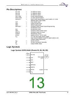
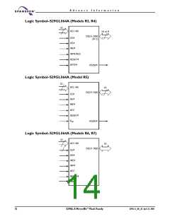
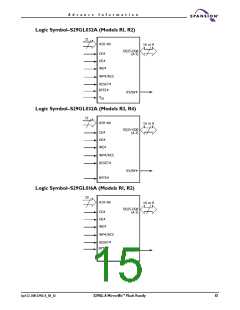
Logic Symbol–S29GL064A (Models R1, R2, R8, R9)
22
A21–A0
16 or 8
DQ15–DQ0
(A-1)
CE#
OE#
WE#
WP#/ACC
RESET#
BYTE#
VIO
RY/BY#
April 22, 2005 S29GL-A_00_A3
S29GL-A MirrorBit™ Flash Family
11

 SPANSION [ SPANSION ]