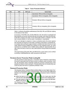
A d v a n c e I n f o r m a t i o n
Logical Inhibit
Write cycles are inhibited by holding any one of OE# = V , CE# = V , or WE#
IL
IH
= V . To initiate a write cycle, CE# and WE# must be a logical zero (V ) while
IH
IL
OE# is a logical one (V ).
IH
Power-Up Write Inhibit
If WE# = CE# = V and OE# = V during power-up, the device does not accept
IL
IH
commands on the rising edge of WE#. The internal state machine is automatically
reset to reading array data on power-up.
VCC and VIO Power-up And Power-down Sequencing
The device imposes no restrictions on V and V power-up or power-down se-
CC
IO
quencing. Asserting RESET# to V is required during the entire V
and V
IO
IL
CC
power sequence until the respective supplies reach their operating voltages.
Once, V and V attain their respective operating voltages, de-assertion of RE-
CC
IO
SET# to V is permitted.
IH
34
S29CD032G
30606B0 March 22, 2004

 SPANSION [ SPANSION ]