SN6A511
LCD Controller with Voice/Dual Tone Melody
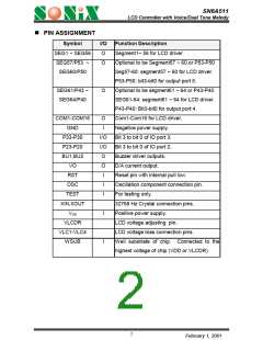
PIN ASSIGNMENT
Symbol
I/O
O
Function Description
SEG1 ~ SEG56
SEG57/P53 ~
SEG60/P50
Segment1~ 56 for LCD driver
Optional to be Segment57 ~ 60 or P53-P50
Seg57-60: segment57 ~ 60 for LCD driver.
P53-P50: bit3-bit0 for output port 5.
Optional to be segment61 ~ 64 or P43-P40
SEG61-64: segment61 ~ 64 for LCD driver.
P43-P40: Bit3-bit0 for output port 4.
Com1-Com16 for LCD driver.
Negative power supply.
O
SEG61/P43 ~
SEG64/P40
O
COM1-COM16
GND
O
I
P33-P30
P23-P20
BU1,BU2
VO
I/O
I/O
O
O
I
Bit 3 to bit 0 of IO port 3.
Bit 3 to bit 0 of IO port 2.
Buzzer driver outputs.
D/A current output.
RST
Reset pin with internal pull low.
Oscillation component connection pin.
For testing only.
OSC
I
TEST
I
XIN,XOUT
VDD
32768 Hz Crystal connection pins.
Positive power supply.
I
I
VLCDR
VLC1-VLC4
WSUB
LCD voltage adjusting pin.
LCD voltage bias connection pins.
Well substrate of chip. Connected to the
highest voltage of chip (VDD or VLCDR).
2
February 1, 2001

 SONIX [ SONIX TECHNOLOGY COMPANY ]