2003/7/8 ver 0.3
SN11088
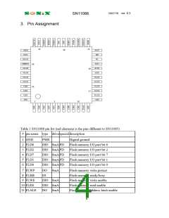
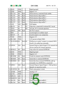
12 GND
PWR
Digital ground
Digital 3.3V
13 VDD
PWR
14 FLCLE
15 FLCE1
16 FLCE3
17 FLCE5
18 FLCE7
19 LED
DO 8mA
DO 8mA
DO 8mA
DO 8mA
DO 8mA
DIO 8mA PD
Flash memory command latch enable
Flash memory chip enable 1
Flash memory chip enable 3
Flash memory chip enable 5
Flash memory chip enable 7
LED lighter
20 RSTN
21 TEST
22 GPIO1
23 XIN
DI
PU
PD
Chip reset, connected to external RC circuit
Test pin, NC in normal operation
Do Not Connect
DI
DIO 8mA
I
-
-
-
-
-
-
Crystal input or oscillator input
Crystal output or no connection
Digital 3.3V
24 XOUT
25 VDD
O
PWR
PWR
26 FLVDD
3.3V power to flash VDD
27 FLPOWERDO 8mA OC
Flash power control, connect to external MOS
Needs to be pulled up externally.
General Purpose Input/Output 0 for internal test
Always pull up for normal operation
Chip select for external EEPROM
28 GPIO0 DIO 8mA
29 ROMCS DO 4mA
30 GND
31 VDD
PWR
PWR
Digital ground
Digital 3.3V
32 ROMSK DO 4mA
33 ROMDI DO 4mA
Clock for external serial EEPROM
Serial data to external EEPROM
34 ROMDO DI
4mA
Serial data from external EEPROM, pull up
externally if no EEPROM is connected
General Purpose Input/Output 1. Pull up/down
depends on operation modes
35 GPIO1 DIO 8mA -
36 FLWPSW DI
PU
Flash write protect switch
37 AVDD
38 AVSS
39 DPLUS
PWR
Analog 3.3V
PWR
AIO
Analog ground
USB D+ signal
USB D- signal
-
-
-
-
40 DMINUS AIO
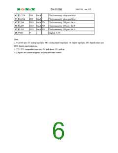
41 FLCE8
42 FLCE6
DO 8mA
DO 8mA
Flash memory chip enable 8
Flash memory chip enable 6
5

 SONIX [ SONIX TECHNOLOGY COMPANY ]