USB MultiSwitchTM Hub
Datasheet
Chapter 11 DC Parameters
11.1
Maximum Guaranteed Ratings
Operating Temperature Range . . . . . . . . . . . . . . . . . . . . . . . . . . . . . . . . . . . . . . . . . . . . . . 0oC to +70oC
Storage Temperature Range. . . . . . . . . . . . . . . . . . . . . . . . . . . . . . . . . . . . . . . . . . . . . . .-55o to +150oC
Lead Temperature Range (soldering, 10 seconds) . . . . . . . . . . . . . . . . . . . . . . . . . . . . . . . . . . . +325oC
Positive Voltage on any I/O pin, with respect to Ground. . . . . . . . . . . . . . . . . . . . . . . . . . . . . . . . . 5.5V
Negative Voltage on any I/O pin, with respect to Ground . . . . . . . . . . . . . . . . . . . . . . . . . . . . . . . . .-0.V
Positive Voltage on XTAL1, with respect to Ground . . . . . . . . . . . . . . . . . . . . . . . . . . . . . . . . . . . . 4.0V
Positive Voltage on XTAL2, with respect to Ground . . . . . . . . . . . . . . . . . . . . . . . . . . . . . . . . . . . . 3.6V
Negative Voltage on XTAL1 and XTAL2, with respect to Ground . . . . . . . . . . . . . . . . . . . . . . . . . . .-0.V
Maximum VDDA33 &VDD33. . . . . . . . . . . . . . . . . . . . . . . . . . . . . . . . . . . . . . . . . . . . . . . . . . . . . . . . +4.0V
*Stresses above the specified parameters could cause permanent damage to the device. This is a
stress rating only and functional operation of the device at any other condition above those indicated
in the operation sections of this specification is not implied.
Note: When powering this device from laboratory or system power supplies, it is important that the
Absolute Maximum Ratings not be exceeded or device failure can result. Some power supplies
exhibit voltage spikes on their outputs when the AC power is switched on or off. In addition,
voltage transients on the AC power line may appear on the DC output. When this possibility
exists, it is suggested that a clamp circuit be used.
11.1.1
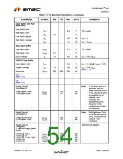
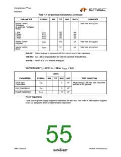
DC Electrical Characteristics
(TA = 0°C - 70°C, VDD33, VDDA33, = +3.3 V tolerance -5% to ±10%)
Table 11.1 DC Electrical Characteristics
PARAMETER
SYMBOL
MIN
TYP
MAX
UNITS
COMMENTS
I, IS Type Input Buffer
Low Input Level
VILI
VIHI
IIL
0.8
V
V
TTL Levels
High Input Level
2.0
-10
250
Input Leakage
+10
350
uA
mV
VIN = 0 to VDD33
Hysteresis (‘IS’ Only)
VHYSI
300
Input Buffer with Pull-Up
(IPU)
Low Input Level
VILI
VIHI
IILL
0.8
V
V
TTL Levels
High Input Level
Low Input Leakage
High Input Leakage
2.0
10
30
uA
uA
VIN = 0
IIHL
VIN = VDD33
SMSC USB2524
Revision 1.91 (08-22-07)
DATA5S3HEET

 SMSC [ SMSC CORPORATION ]