Integrated USB 2.0 Compatible 7-Port Hub
Datasheet
Chapter 7 DC Parameters
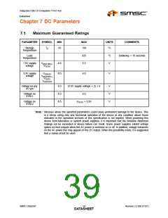
7.1
Maximum Guaranteed Ratings
PARAMETER
SYMBOL
MIN
MAX
UNITS
COMMENTS
Storage
Temperature
TA
-55
150
°C
Lead
325
2.5
°C
V
Soldering < 10 seconds
Temperature
1.8V supply
voltage
VDDA18PLL
VDD18
-0.5
-0.5
3.3V supply
voltage
VDDA33
VDDA33PLL
VDD33
4.0
V
VDD33CR
Voltage on any
I/O pin
-0.5
-0.5
-0.5
(3.3V supply voltage + 2) ≤ 6
V
V
V
Voltage on
XTAL1
4.0
Voltage on
XTAL2
VDD18 + 0.3V
Note: Stresses above the specified parameters could cause permanent damage to the device. This
is a stress rating only and functional operation of the device at any condition above those
indicated in the operation sections of this specification is not implied. When powering this
device from laboratory or system power supplies, it is important that the Absolute Maximum
Ratings not be exceeded or device failure can result. Some power supplies exhibit voltage
spikes on their outputs when the AC power is switched on or off. In addition, voltage transients
on the AC power line may appear on the DC output. When this possibility exists, it is suggested
that a clamp circuit be used.
SMSC USB2507
Revision 2.3 (08-27-07)
DATA3S9HEET

 SMSC [ SMSC CORPORATION ]