Legacy-Free Keyboard/Embedded Controller with SPI and LPC Docking Interface
Chapter 3 Functional Description
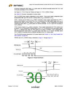
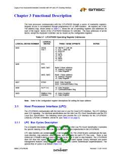
The host processor communicates with the LPC47N350 through a series of read/write registers.
Register access is accomplished through programmed I/O or DMA transfers. All registers are 8 bits.
The address map, shown below in Table 3.1, shows the set of operating registers and addresses for
each of the logical blocks of the LPC47N350 Notebook I/O controller. The base addresses of all the
blocks, except the Keyboard Controller can be moved via the configuration registers.
Table 3.1 LPC47N350 Operating Register Addresses
LOGICAL
LOGICAL DEVICE NUMBER
DEVICE
FIXED / BASE OFFSETS
NOTES
0x04
Serial
+0: RB/TB LSB div
Port 1
+1: IER MSB div
+2: IIR/FCR
+3: LCR
+4: MCR
+5: LSR
+6: MSR
+7: SCR
0x06
RTC
0x60, 0x61
Bank 0 Base address
+0: Address Register
+1: Data Register *
0x62, 0x63
Bank 1 Base address
+0: Address Register
+2: Data Register *
0x07
0x08
0x09
KYBD
0x60: Data Register
0x64: Command/Status Reg.
ACP1 EC
+0: Data Register
+1: Command/Status Reg.
Mailbox Reg.
Interface
+0: Index Register
+1: Data Register.
Note: Refer to the configuration register descriptions for setting the base address
3.1
Host Processor Interface (LPC)
The LPC47N350 communicates with the host over a Low Pin Count (LPC) interface. The LPC interface
uses 3.3V signaling. For electrical specifications see the Intel Low Pin Count Specification and the PCI
Local Bus Specification. The following seven pins provide the LCP interface for the LPC47N350:
LAD[3:0], LPCPD#, LFRAME#, LRESET#. (see Table 2.2 on page 4).
3.1.1
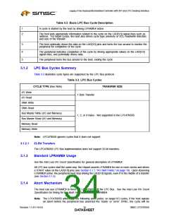
LPC Bus Cycles Description
For a complete description of the LPC Bus Cycles see the Intel Low Pin Count Specification. It provides
the specific tailoring of the Intel Low Pin Count Specification implemented in the LPC47N350.
LPC data transfers are serialized over a 4-bit bus, LAD[3:0]. The LAD[3:0] pins communicate the type,
cycle direction, chip selection, address, data, and wait states for each LPC Bus cycle. There is one
control pin LFRAME# which is used exclusively by the host to start or stop transfers. The LPC47N350
does not drive this signal. Optionally implemented side-band signals convey interrupts and power
management features using the same signals found on current motherboard implementations. The
general flow of cycles is as follows (Table 3.2):
SMSC LPC47N350
Revision 1.1 (01-14-03)
DATA1S5HEET

 SMSC [ SMSC CORPORATION ]