Non-PCI Single-Chip Full Duplex Ethernet Controller
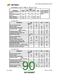
CAPACITANCE TA = 25°C; fc = 1MHz; VCC = 5V, or VCC = +3.3V
LIMITS
TYP
5
PARAMETER
Clock Input Capacitance
(XTAL1)
Clock Output Capacitance
(XTAL2)
SYMBOL
MIN
MAX
6
UNIT
pF
TEST CONDITION
All pins except pin
under test tied to AC
ground
CCIN
CCOUT
5
6
pF
Input Capacitance
Output Capacitance
CIN
COUT
10
20
pF
pF
VCC = 5V +/- 10%
PARAMETER
MIN
10BASE-T
TYP
MAX
UNITS
Receiver Threshold Voltage
Receiver Squelch
Receiver Common Mode Range
Transmitter Output: Voltage
100
400
mV
mV
300
0
±2
585
VDD
±3
±2.5
V
ohms
mV
mV
V
Source Resistance
10
Transmitter Output DC Offset
Transmitter Backswing Voltage to Idle
Differential Input Voltage
50
100
±3
±0.585
AUI
Receiver Threshold Voltage
Receiver Squelch
Receiver Common Mode Range
Transmitter Output Voltage (R=78Ω)
Transmitter Backswing Voltage to Idle
Input Differential Voltage
60
240
mV
mV
180
0
300
VDD
±1.2
±0.45
±0.85
V
mV
V
mA
mV
100
±0.3
±1.2
±150
±40
Output Short Circuit (to VCC or GND) Current
Differential Idle Voltage (measured 8.0 µs after
last positive transition of data frame)
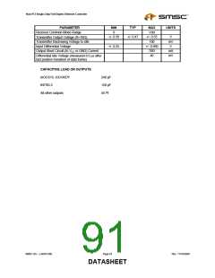
VCC = 3.3V +/- 10%
PARAMETER
MIN
10BASE-T
TYP
MAX
UNITS
Receiver Threshold Voltage
Receiver Squelch
Receiver Common Mode Range
TBD
260
mV
mV
225
0
+/- 1.3
520
Vdd
+/- 1.6
10
50
100
Transmitter Output:
Voltage
Source Resistance
+/- 1.5
V
ohms
mV
mV
V
Transmitter Output DC Offset
Transmitter Backswing Voltage to Idle
Differential Input Voltage
+/- 0.520
AUI
+/- 3
Receiver Threshold Voltage
Receiver Squelch
TBD
140
mV
mV
120
160
Rev. 11/18/2004
Page 90
SMSC DS – LAN91C96I
DATASHEET

 SMSC [ SMSC CORPORATION ]