Highly Efficient Single-Chip 10/100 Non-PCI Ethernet Controller
Datasheet
5.2.2
TX FIFO Ports
The TX data Path consists of two FIFOs, the TX status and data. The TX Status FIFO can be read
from two locations. The TX Status FIFO Port will perform a destructive read, thus “Popping” the data
from the TX Status FIFO. There is also the TX Status FIFO PEEK location. This location allows a non-
destructive read of the top (oldest) location of the FIFO.
The TX data FIFO is Write Only. It is aliased in 8 DWORD locations (16 WORD locations in 16-bit
mode) from the 20h offset to 3Ch offset. The host may write to any of the 8(16) locations since they
all access the same TX data FIFO location and perform the same function.
5.3
System Control and Status Registers
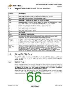
Table 5.1, "LAN9116 Direct Address Register Map", lists the registers that are directly addressable by
the host bus.
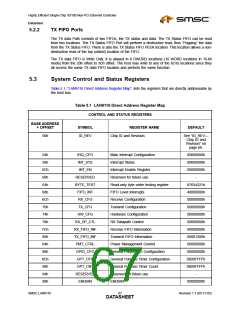
Table 5.1 LAN9116 Direct Address Register Map
CONTROL AND STATUS REGISTERS
BASE ADDRESS
+ OFFSET
SYMBOL
REGISTER NAME
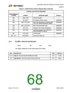
Chip ID and Revision.
DEFAULT
50h
ID_REV
See “ID_REV—
Chip ID and
Revision” on
page 68.
54h
58h
5Ch
60h
64h
68h
6Ch
70h
74h
78h
7Ch
80h
84h
88h
8Ch
90h
94h
98h
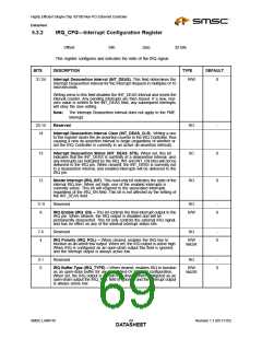
IRQ_CFG
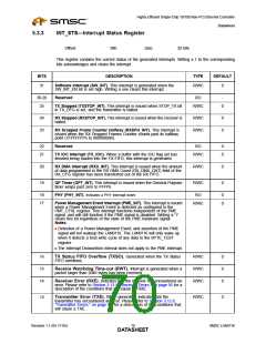
INT_STS
Main Interrupt Configuration
Interrupt Status
00000000h
00000000h
00000000h
-
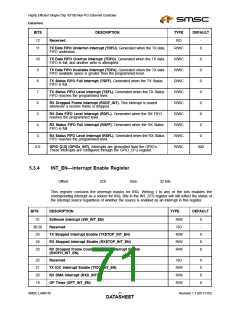
INT_EN
Interrupt Enable Register
Reserved for future use
Read-only byte order testing register
FIFO Level Interrupts
RESERVED
BYTE_TEST
FIFO_INT
87654321h
48000000h
00000000h
00000000h
00000800h
00000000h
00000000h
00001200h
00000000h
00000000h
0000FFFFh
0000FFFFh
-
RX_CFG
Receive Configuration
TX_CFG
Transmit Configuration
HW_CFG
Hardware Configuration
RX Datapath Control
RX_DP_CTL
RX_FIFO_INF
TX_FIFO_INF
PMT_CTRL
GPIO_CFG
GPT_CFG
GPT_CNT
RESERVED
ENDIAN
Receive FIFO Information
Transmit FIFO Information
Power Management Control
General Purpose IO Configuration
General Purpose Timer Configuration
General Purpose Timer Count
Reserved for future use
ENDIAN
00000000h
SMSC LAN9116
Revision 1.1 (05-17-05)
DATA6S7HEET

 SMSC [ SMSC CORPORATION ]