Highly Efficient Single-Chip 10/100 Non-PCI Ethernet Controller
Datasheet
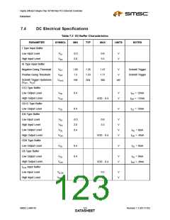
Table 7.4 100BASE-TX Tranceiver Characteristics
PARAMETER
SYMBOL
MIN
TYP
MAX
UNITS
NOTES
Peak Differential Output Voltage
High
V
950
-
1050
mVpk
Note 7.4
PPH
Peak Differential Output Voltage
Low
V
-950
-
-1050
mVpk
Note 7.4
PPL
Signal Amplitude Symmetry
Signal Rise & Fall Time
Rise & Fall Time Symmetry
Duty Cycle Distortion
Overshoot & Undershoot
Jitter
V
98
3.0
-
-
-
102
5.0
0.5
65
%
nS
nS
%
Note 7.4
Note 7.4
Note 7.4
Note 7.5
SS
T
RF
T
-
RFS
D
35
-
50
-
CD
OS
V
5
%
1.4
nS
Note 7.6
Note 7.4 Measured at the line side of the transformer, line replaced by 100Ω (+/- 1%) resistor.
Note 7.5 Offset from16 nS pulse width at 50% of pulse peak
Note 7.6 Measured differentially.
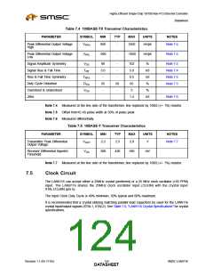
Table 7.5 10BASE-T Tranceiver Characteristics
PARAMETER
SYMBOL
MIN
TYP
MAX
UNITS
NOTES
Transmitter Peak Differential
Output Voltage
V
2.2
2.5
2.8
V
Note 7.7
OUT
Receiver Differential Squelch
Threshold
V
300
420
585
mV
DS
Note 7.7 Measured at the line side of the transformer, line replaced by 100Ω (+/- 1%) resistor.
7.5
Clock Circuit
The LAN9116 can accept either a 25MHz crystal (preferred) or a 25 MHz clock oscillator (±50 PPM)
input. The LAN9116 shares the 25MHz clock oscillator input (CLKIN) with the crystal input
XTAL1/CLKIN (pin 6).
The Input Clock Duty Cycle is 40% minimum, 50% typical and 60% maximum.
It is recommended that a crystal utilizing matching parallel load capacitors be used for the LAN9116
crystal input/output signals (XTAL1, XTAL2). See Table 7.6, "LAN9116 Crystal Specifications" for crystal
specifications.
Revision 1.1 (05-17-05)
124
SMSC LAN9116
DATASHEET

 SMSC [ SMSC CORPORATION ]