±15kV ESD Protected MII/RMII 10/100 Ethernet Transceiver with HP Auto-MDIX Support and flexPWR® Technology in a Small Footprint
Datasheet
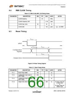
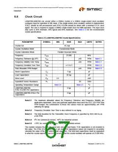
6.6
Clock Circuit
LAN8700/LAN8700i can accept either a 25MHz crystal or a 25MHz single-ended clock oscillator
(±50ppm) input for operation in MII mode. If the single-ended clock oscillator method is implemented,
XTAL2 should be left unconnected and XTAL1/CLKIN should be driven with a nominal 0-3.3V clock
signal. The user is required to supply a 50MHz single-ended clock for RMII operation. The input clock
duty cycle is 40% minimum, 50% typical and 60% maximum. See Table 6.12 for the recommended
crystal specifications.
Table 6.12 LAN8700/LAN8700i Crystal Specifications
PARAMETER
SYMBOL
MIN
NOM
AT, typ
Fundamental Mode
Parallel Resonant Mode
MAX
UNITS
NOTES
Crystal Cut
Crystal Oscillation Mode
Crystal Calibration Mode
Frequency
F
-
25.000
-
MHz
PPM
PPM
PPM
PPM
pF
fund
o
Frequency Tolerance @ 25 C
Frequency Stability Over Temp
Frequency Deviation Over Time
Total Allowable PPM Budget
Shunt Capacitance
F
-
-
±50
Note 6.1
Note 6.1
Note 6.2
Note 6.3
tol
F
-
-
±50
temp
F
-
+/-3 to 5
-
age
-
-
±50
C
-
7 typ
-
O
Load Capacitance
C
-
20 typ
-
pF
L
Drive Level
P
0.5
-
-
mW
Ohm
W
Equivalent Series Resistance
Operating Temperature Range
R
-
-
-
30
Note 6.5
-
1
o
Note 6.4
-
C
LAN8700/LAN8700i
XTAL1/CLKIN Pin Capacitance
3 typ
pF
pF
LAN8700/LAN8700i XTAL2 Pin
Capacitance
-
3 typ
-
Note 6.1 The maximum allowable values for Frequency Tolerance and Frequency Stability are
application dependant. Since any particular application must meet the IEEE ±50 PPM Total
PPM Budget, the combination of these two values must be approximately ±45 PPM
(allowing for aging).
Note 6.2 Frequency Deviation Over Time is also referred to as Aging.
Note 6.3 The total deviation for the Transmitter Clock Frequency is specified by IEEE 802.3u as
±100 PPM.
o
o
Note 6.4 0 C for commercial version, -40 C for industrial version.
o
o
Note 6.5 +70 C for commercial version, +85 C for industrial version.
This number includes the pad, the bond wire and the lead frame. PCB capacitance is not included in
this value. The XTAL1/CLKIN pin, XTAL2 pin and PCB capacitance values are required to accurately
calculate the value of the two external load capacitors. The total load capacitance must be equivalent
to what the crystal expects to see in the circuit so that the crystal oscillator will operate at 25.000 MHz.
SMSC LAN8700/LAN8700i
Revision 2.3 (04-12-11)
DATA6S7HEET

 SMSC [ SMSC CORPORATION ]