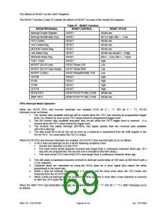
The IrDA V1.1 (FIR) and Consumer IR formats are driven by the SCE registers. Descriptions of these registers can
be found in the SMSC Infrared Communications Controller Specification. The Base Address for the SCE registers is
programmed in CR2B, the SCE Base Address Register (see section CR28 on page 111).
IrDA SIR/FIR and ASKIR
IrDA SIR (v1.0) specifies asynchronous serial communication at baud rates up to 115.2Kbps. Each byte is sent
serially LSB first beginning with a zero value start bit. A zero is signaled by sending a single infrared pulse at the
beginning of the serial bit time. A one is signaled by the absence of an infrared pulse during the bit time. Please refer
to section AC TIMING for the parameters of these pulses and the IrDA waveforms.
IrDA FIR (v1.1) includes IrDA v1.0 SIR and additionally specifies synchronous serial communications at data rates up
to
4Mbps.
Data
is
transferred
LSB
first
in
packets that can be up to 2048 bits in length. IrDA v1.1 includes .576Mbps and 1.152Mbps data rates using an
encoding scheme that is similar to SIR. The 4Mbps data rate uses a pulse position modulation (PPM) technique.
The ASKIR infrared allows asynchronous serial communication at baud rates up to 19.2Kbps. Each byte is sent
serially LSB first beginning with a zero value start bit. A zero is signaled by sending a 500KHz carrier waveform for
the duration of the serial bit time. A one is signaled by the absence of carrier during the bit time. Please refer to
section AC TIMING for the parameters of the ASKIR waveforms.
Consumer IR
The FDC37N769 Consumer IR interface is a general-purpose Amplitude Shift Keyed encoder/decoder with
programmable carrier and bit-cell rates that can emulate many popular TV Remote encoding formats; including,
38KHz PPM, PWM and RC-5. The carrier frequency is programmable from 1.6MHz to 6.25KHz. The bit-cell rate
range is 100KHz to 390Hz.
Hardware Interface
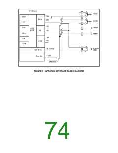
The FDC37N769 IR hardware interface is shown in FIGURE 3. This interface supports two types of external FIR
transceiver modules. One uses a mode pin (IR Mode) to program the data rate, while the other has a second Rx data
pin (IRR3). The FDC37N769 uses Pin 21 for these functions. Pin 21 has IR Mode and IRR3 as its first and second
alternate function, respectively. These functions are selected through CR29 as shown in Table 60.
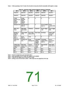
Table 60 - FIR Transceiver Module-Type Select
HP MODE1
FUNCTION
0
1
IR Mode
IRR3
Note1
HPMODE is CR29, BIT 4 (see section CR29 on page 112). Refer to the Infrared Interface Block
Diagram on the following page for HPMODE implementation.
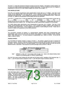
The FAST bit is used to select between the SIR mode and FIR mode receiver, regardless of the transceiver type. If
FAST = 1, the FIR mode receiver is selected; if FAST = 0, the SIR mode receiver is selected (Table 61).
Table 61 - IR Rx Data Pin Selection
CONTROL SIGNALS
INPUTS
FAST
HPMODE
RX1
RX2
0
X
1
X
0
1
RX1=RXD2
RX2=IRRX2
RX1=RXD2
RX1=IR Mode/IRR3
RX2=IRRX2
RX2=IR Mode/IRR3
data is loaded into the transmit buffer while a character
is being received, the transmission will not start until the
last bit has been received and the time-out expires. If
the start bit of another character is received during this
time-out, the timer is restarted after the new character is
received. The Half Duplex Time-out is programmable
from 0 to 25.5ms in 100µs increments (see section
IR Half Duplex Turnaround Delay Time
If the Half Duplex option is chosen there is an IR Half
Duplex Time-out that constrains IRCC direction mode
changes. This time-out starts as each bit is transferred
and prevents direction mode changes until the time-out
expires. The timer is restarted whenever new data
arrives in the current direction mode. For example, if
CR2D on page 113).
SMSC DS – FDC37N769
Page 73 of 138
Rev. 12/21/2000

 SMSC [ SMSC CORPORATION ]