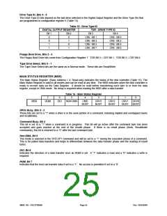
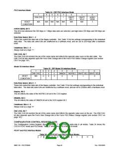
PS/2 Interface Mode
Table 24 - DIR PS/2 Interface Mode
7
6
1
5
1
4
1
3
1
2
1
0
DSK CHG
DRATE
DRATE
nHIGH
SEL1
SEL0
DENS
RESET
N/A
N/A
N/A
N/A
N/A
N/A
N/A
1
CONDITION
nHIGH DENS, Bit 0
This bit is low whenever the 500 Kbps or 1 Mbps data rates are selected, and high when 250 Kbps and 300 Kbps are
selected.
Data Rate Select, Bits 1 - 2
These bits control the data rate of the floppy controller. See Table 19 for the settings corresponding to the individual
data rates. The data rate select bits are unaffected by a software reset, and are set to 250 Kbps after a hardware
reset.
Undefined, Bits 3 - 6
Always read as a logic “1”
DSK CHG, Bit 7
The DSK CHG bit monitors the pin of the same name and reflects the opposite value seen on the disk cable. The
DSK CHG bit also depends upon the Force Disk Change bits in the Force FDD Status Change register (see section
CR17 on page 107).
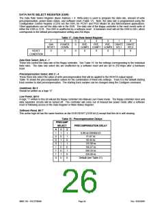
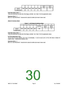
Model 30 Interface Mode
Table 25 - DIR Model 30 Interface Mode
7
6
0
0
5
0
0
4
0
0
3
DMAEN
0
2
1
0
DSK CHG
N/A
NOPREC DRATE SEL1 DRATE SEL0
RESET
CONDITION
0
1
0
Data Rate Select, Bits 0 - 1
These bits control the data rate of the floppy controller. See Table 19 for the settings corresponding to the individual
data rates. The data rate select bits are unaffected by a software reset, and are set to 250kb/s after a hardware reset
Noprec, Bit 2
This bit reflects the value of the NOPREC bit set in the CCR register.
DMAEN, Bit 3
This bit reflects the value of DMAEN bit set in the DOR register bit 3.
Undefined, Bits 4 - 6
Always read as a logic “0”
DSK CHG, Bit 7
The DSK CHG bit monitors the pin of the same name and reflects the opposite value seen on the pin. The DSK CHG
bit also depends upon the Force Disk Change bits in the Force FDD Status Change register (see section CR17 on
page 107).
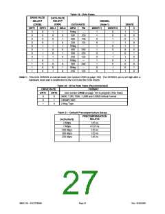
CONFIGURATION CONTROL REGISTER (CCR)
The Configuration Control Register (Bass Address + 7: Write-only) is write-only in all modes. Table 26 shows the
CCR in PC/AT mode and PS/2 mode. Table 27 shows the CCR in Model 30 mode.
PC/AT and PS/2 Interface Modes
Table 26 - CCR PC/AT and PS/2 Interface Modes
7
6
5
4
3
2
1
0
SMSC DS – FDC37N3869
Page 29
Rev. 10/25/2000

 SMSC [ SMSC CORPORATION ]