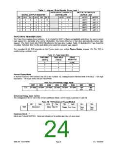
DATA REGISTER (FIFO)
The Data Register (Base Address + 5) is used to transfer all command parameter information, disk data and result
status between the host processor and the floppy disk controller. The Data Register is Read/Write. Data transfers are
governed by the RQM and DIO bits in the Main Status Register.
The Data Register defaults to FIFO disabled mode after any form of reset. This maintains PC/AT hardware
compatibility. The default values can be changed through the Configure command (enable full FIFO operation with
threshold control). The advantage of the FIFO is that it allows the system a larger DMA latency without causing
disk error.
a
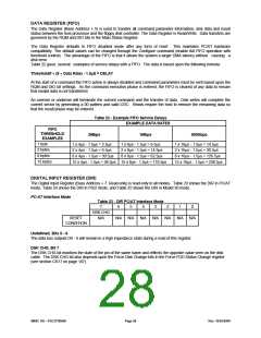
Table 22 gives several examples of service delays with a FIFO. The data is based upon the following formula:
Threshold# × (8 ÷ Data Rate) - 1.5µS = DELAY
At the start of a command the FIFO action is always disabled and command parameters must be sent based upon the
RQM and DIO bit settings. As the command execution phase is entered, the FIFO is cleared of any data to ensure
that invalid data is not transferred.
An overrun or underrun will terminate the current command and the transfer of data. Disk writes will complete the
current sector by generating a 00 pattern and valid CRC. Reads require the host to remove the remaining data so
that the result phase may be entered.
Table 22 - Example FIFO Service Delays
EXAMPLE DATA RATES
FIFO
THRESHOLD
2Mbps
1Mbps
500Kbps
EXAMPLES
1 byte
1 x 4µs - 1.5µs = 2.5µs
2 x 4µs - 1.5µs = 6.5µs
8 x 4µs - 1.5µs = 30.5µs
1 x 8µs - 1.5µs = 6.5µs
2 x 8µs - 1.5µs = 14.5µs
8 x 8µs - 1.5µs = 62.5µs
1 x 16µs - 1.5µs = 14.5µs
2 x 16µs - 1.5µs = 30.5µs
8 x 16µs - 1.5µs = 126.5µs
15 x 16µs - 1.5µs = 238.5µs
2 bytes
8 bytes
15 bytes
15 x 4µs - 1.5µs = 58.5µs 15 x 8µs - 1.5µs = 118.5µs
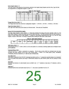
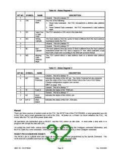
DIGITAL INPUT REGISTER (DIR)
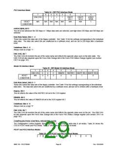
The Digital Input Register (Bass Address + 7: Read-only) is read-only in all modes. Table 23 shows the DIR in PC/AT
mode, Table 24 shows the DIR in PS/2 mode, and Table 25 shows the DIR in Model 30 mode.
PC-AT Interface Mode
Table 23 - DIR PC/AT Interface Mode
7
6
5
4
3
2
1
0
DSK CHG
N/A
RESET
CONDITION
N/A
N/A
N/A
N/A
N/A
N/A
N/A
Undefined, Bits 0 - 6
The data bus outputs D0 - 6 will remain in a high impedance state during a read of this register.
DSK CHG, Bit 7
The DSK CHG bit monitors the state of the pin of the same name and reflects the opposite value seen on the disk
cable. The DSK CHG bit also depends upon the Force Disk Change bits in the Force FDD Status Change register
(see section CR17 on page 107).
SMSC DS – FDC37N3869
Page 28
Rev. 10/25/2000

 SMSC [ SMSC CORPORATION ]