used to select which of the Configuration
Registers are to be accessed at port 3F1H
(371H).
Configuration Register Description
The configuration registers consist of the
Configuration Select Register (CSR) and
Configuration Registers CR-00 -CR-29. The
configuration select register is written to by
29
Configuration Registers CR00 -CR
These registers are set to their default values at
power up and are not affected by RESET
(except where explicitly defined that a hardware
reset causes that bit to be reset to default). They
are accessed at port 3F1H (or 371H). Refer to
the following descriptions for the function of
each configuration register.
writing to port 3F0H (or 370H).
The
Configuration Registers CR-00; CR-29 are
accessed by reading or writing to port 3F1H (or
371H).
Configuration Select Register (CSR)
This register can only be accessed when the
chip is in the Configuration Mode. This register,
located at port 3F0H (370H), must be initialized
upon entering the Configuration Mode before the
configuration registers can be accessed and is
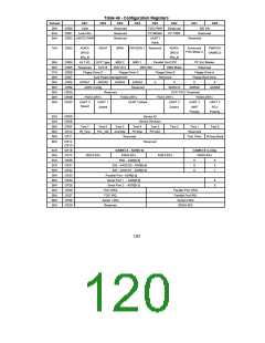
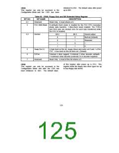
CR00
This register can only be accessed when the
chip is in the Configuration Mode and after the
CSR has been initialized to 00H. The default
value of this register after power up is 28H.
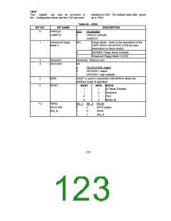
Table 47 - CR00
BIT NO.
BIT NAME
DESCRIPTION
0, 1
IDE ENABLE/
Bits (Note 1)
10
Alternate
Function
00 - IDE, IRRX2, IRTX2, IRQ_H disabled (Default)
01 - Reserved (IDE, IRRX2, IRTX2, IRQ_H disabled)
10 - IDE Enabled
11 - IRRX2, IRTX2, IRQ_H Enabled
Read only. Read as 0
2
3
Reserved
FDC Power (see A high level on this bit, supplies power to the FDC (default). A
note _PWRDN)
Reserved
Valid
low level on this bit puts the FDC in low power mode.
4,5,6
7
Read only. A read returns bit 5 as a 1 and bits 4 and 6 as a 0.
A high level on this software controlled bit can be used to
indicate that a valid configuration cycle has occurred. The
control software must take care to set this bit at the appropriate
times. Set to zero after power up. This bit has no effect on any
other hardware in the chip.
Note 1: When "0x" is selected, 30ua pull-ups are active on the "nIDEEN, nHDCS0 and nHDCS1
pins", at all other times, the pull-ups are disabled.
When "11" is selected, IRQ_H is available as an IRQ output, and IRRX2 and IRTX2 are
available as alternate IR pins (pull-ups disabled). When "10" is selected, nIDEEN, nHDCS0
and nHDCS1 are used to control the IDE interface (pull-ups disabled).
121

 SMSC [ SMSC CORPORATION ]