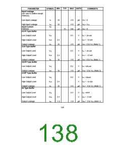
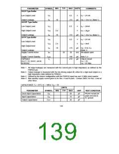
MIN
TYP
MAX UNITS
PARAMETER
SYMBOL
COMMENTS
24
OD Type Buffer
Low Output Level
Output Leakage
VOL
IOL
0.5
V
IOL =
24 mA
-10
+10
µA VIN = 0 to VCC (Note 1)
24
OD P Type Buffer
Low Output Level
High Output Level
Output Leakage
VOL
VOH
IOL
0.5
V
V
IOL
IOH
=
=
24mA
2.4
-10
-30 A
m
+10
µA
V
VIN = 0 to VCC (Note 1)
24
OP Type Buffer
VOL
VOH
IOL
IOL
=
=
0.5
24 mA
Low Output Level
High Output level
2.4
-10
V
IOH
-4mA
+10
µA VIN = 0 to VCC
(Note 1)
Output Leakage
Supply Current Active
ICC
25
35
mA All outputs open.
Supply Current Standby
ChiProtect
(SLCT, PE, BUSY, nACK,
nERROR)
ICSBY
IIL
100
±10
µA Note 3, 4
µA Chip in circuit:
VCC = 0V
VIN = 6V Max.
Note 1: All output leakages are measured with the current pins in high impedance as defined by the
PWRGD pin.
Note 2: Output leakage is measured with the low driving output off, either for a high level output or a
high impedance state defined by PWRGD.
Note 3: Defined by the device configuration with the PWRGD input low
.
and 14 MHz clock inactive
Note 4: Max standby supply current given is for Rev. H and K parts. Contact SMSC for Rev. J and all
other Revs.
CAPACITANCE TA = 25°C; fc = 1MHz; VCC
=
5V
LIMITS
TYP
PARAMETER
Clock Input Capacitance
Input Capacitance
SYMBOL
CIN
MIN
MAX
20
UNIT
pF
TEST CONDITION
All pins except pin
under test tied to
AC ground
CIN
10
pF
Output Capacitance
COUT
20
pF
139

 SMSC [ SMSC CORPORATION ]